

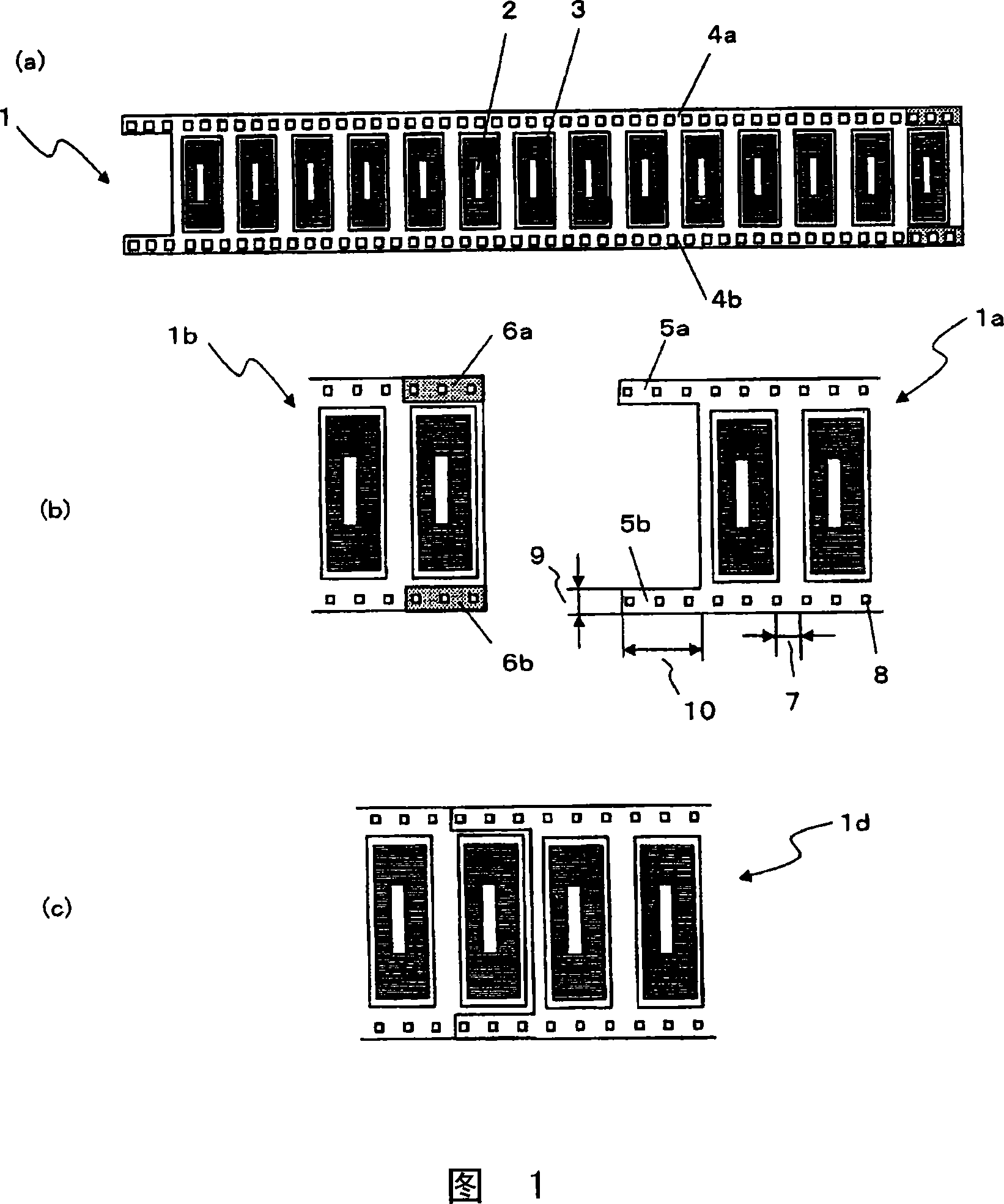
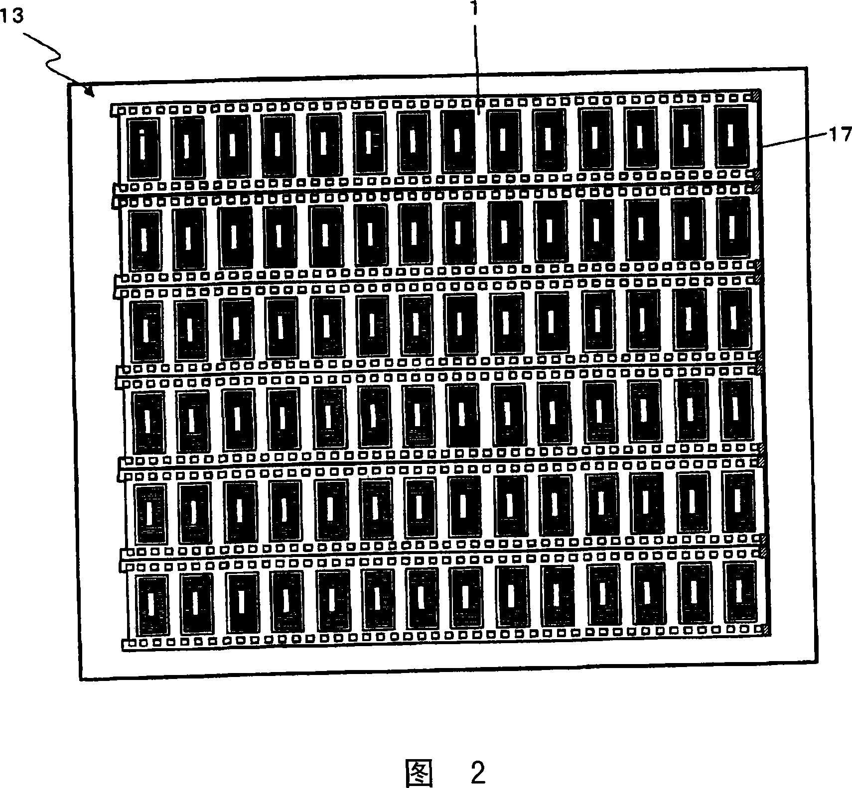
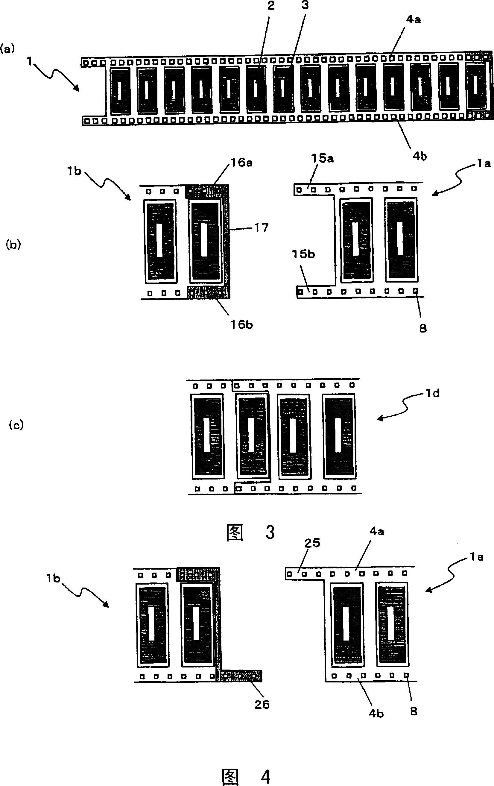
Long film circuit board, and production method and production device therefor
A technology for circuit substrates and manufacturing methods, applied in the directions of printed circuit manufacturing, printed circuits, printed circuits, etc., can solve problems such as difficulty in implementation, difficulty in achieving riveting ease and heat resistance at the same time, and achieve reduced loss, reliable bonding, and easy handling. Effect
- Summary
- Abstract
- Description
- Claims
- Application Information
AI Technical Summary
Problems solved by technology
Method used
Image

Examples
Embodiment 1
[0258] As the base film constituting the flexible film substrate, a long polyimide film (“Capton” 150EN (trade name) manufactured by Toray Dupon Co., Ltd.) with a thickness of 25 μm was prepared. A 15-nm-thick chromium:nickel = 5.95 (weight ratio) alloy layer and a 150-nm-thick copper layer were sequentially laminated on the polyimide film by a roll-to-roll sputtering apparatus for processing long thin films.
[0259] On soda lime glass (thickness 1.1 mm, 300×350 mm) as a support plate, a peelable organic substance was coated with a die coater, and dried at 80° C. for 2 minutes. As the detachable organic matter, a UV-curable adhesive "SK Dyne" SW-22 (manufactured by Soken Chemical Co., Ltd.) and hardener L45 (manufactured by Soken Chemical Co., Ltd.) were used in a ratio of 100:3 (by weight). ) mixed substances. The thickness of the peelable organic layer after drying was 2 μm. Next, an air-blocking film (a polyester film provided with a silicone resin layer for easy parting...
Embodiment 2
[0276] A long thin film circuit board was produced in the same manner as in Example 1 except that the resin was applied over the entire width of the conveying space in the direction perpendicular to the conveying direction at a length of 0.4 mm in the conveying direction.
[0277] The connection strength was measured in the same manner as in Example 1, and it was 13N, which is sufficient strength for transportation in the subsequent process.
Embodiment 3
[0279] A long thin film circuit board was produced in the same manner as in Example 1 except that the temperature of the head of the heating and pressing mechanism 416 was set at 200°C.
[0280] When the connection strength was measured in the same manner as in Example 1, it was 4.7N, which has strength of the level used in the subsequent process. However, there is a concern that there may be a slight shortage when force is applied for intermittent feeding or the like.
PUM
 Abstract
Description
Claims
Application Information