Manufacturing method for LED module

A technology for light-emitting diodes and a manufacturing method, which is applied in the manufacturing of semiconductor/solid-state devices, electrical components, circuits, etc., can solve the problems of easy falling off of identification materials, easy falling off of marking stickers, and low cost of labeling

Inactive Publication Date: 2007-10-03
UNITY OPTO TECH CO LTD
View PDF0 Cites 14 Cited by
  • Summary
  • Abstract
  • Description
  • Claims
  • Application Information

AI Technical Summary

Problems solved by technology

[0003] In the process of printing electronic component symbols on circuit boards in the prior art, the manufacturer needs to have a circuit board printing machine for printing barcodes, serial numbers and other related materials on the circuit board, while manufacturers without circuit board printing machines use manual printing. Paste various marking stickers in different ways, although these two methods can make the circuit board easy to identify, but these two methods need to spend a lot of marking costs; and use the identification data printed by the circuit board printing machine , after a period of time, the identification data is easy to fall off; and those who use manual methods to paste various mark stickers, in addition to the easy fall off of the mark stickers, are more prone to errors due to manual negligence

Method used


Image

  • Manufacturing method for LED module
  • Manufacturing method for LED module

Examples


Embodiment Construction

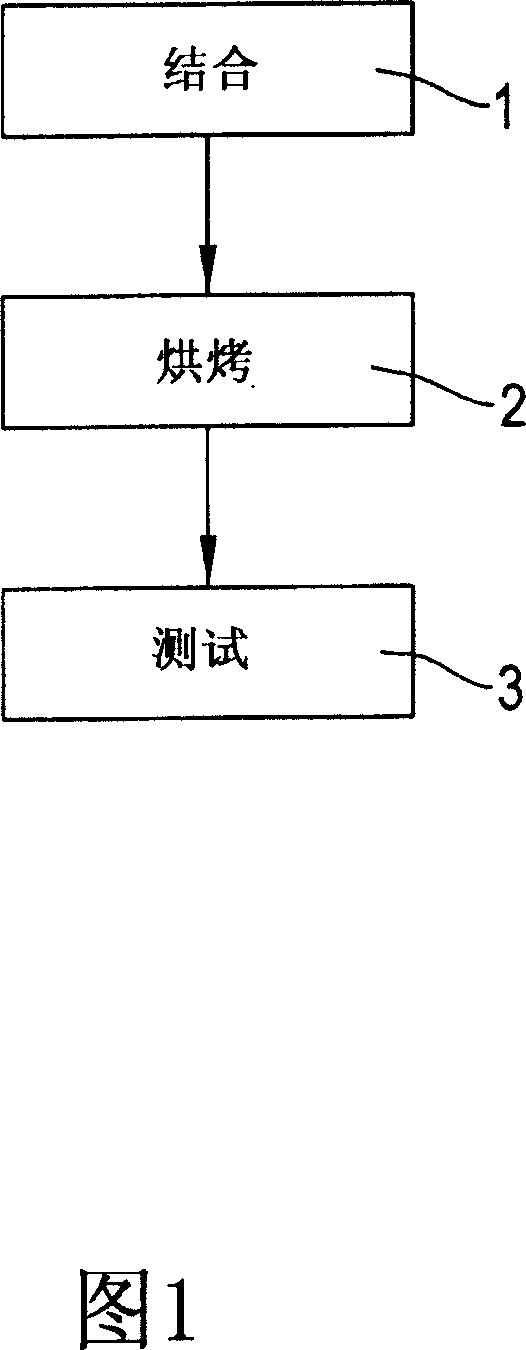
[0019] Referring to Fig. 1, the process of the present invention comprises the following steps:

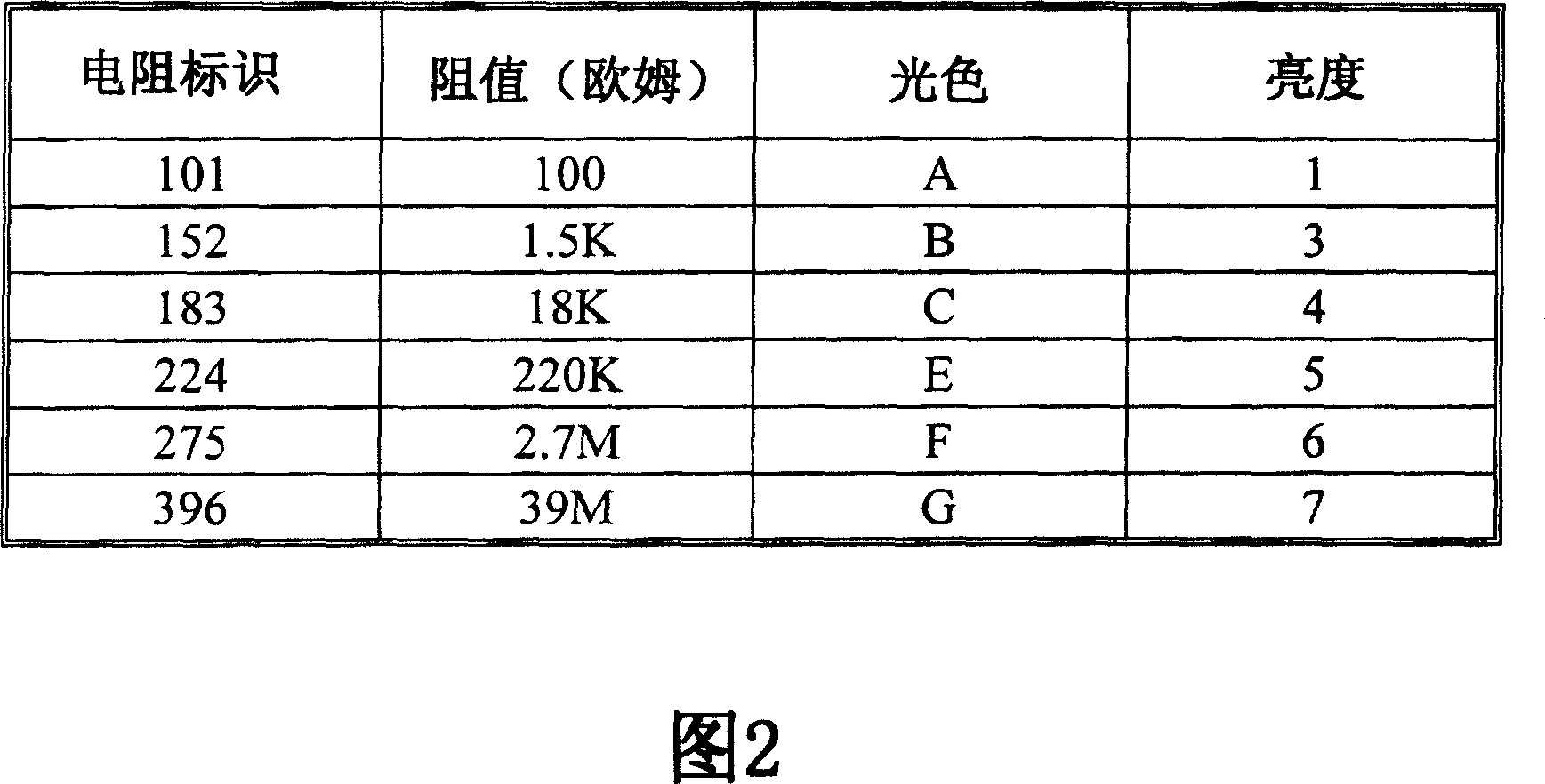
[0020] 1. Combination: The electronic components are combined on the circuit board, and the identification resistor is combined on the side of the light-emitting diode.

[0021] 2. Baking: Place the completed combined circuit board into a reflow oven for baking.

[0022] 3. Test: test the baked circuit board.

[0023] In actual manufacturing, there are two ways for the circuit board to be combined with electronic components, one is the way of plugging in DIP (Dual In-Line Package), and the other is the way of applying solder paste on the circuit board to make the circuit board contacts There is solder on the surface, and the electronic components are combined with the circuit board by using the surface mount technology SMT (Surface Mount Technology). Put it into a reflow oven and bake at high temperature. The baked circuit board is then subjected to a lighting test, a burn-in te...


PUM


Abstract

The present invention relates to a method for preparing light-emitting diode module. Said method mainly includes the following steps: (1), combination: combining electronic element on the circuit board, and combining identification resistor by light-emitting diode; (2), baking: placing the circuit board on which the above-mentioned combination step is completed into a backwelding oven and baking; (3), test: testing the above-mentioned baked circuit board.

Description

technical field [0001] The present invention aims to provide a method for manufacturing a light-emitting diode module that is convenient for identification and can reduce marking costs, and is especially suitable for identifying electronic components such as light-emitting diodes used in circuit boards. Background technique [0002] Due to the rapid development of science and technology, modern people are equipped with a variety of electronic products. However, each electronic product cannot be separated from the design of the circuit board. The general electronic product manufacturing process is nothing more than designing the circuit diagram first, and then marking the electronic components in the circuit diagram. Printing on the circuit board means that the electronic components can be combined with the circuit board, and the completed circuit board is then subjected to a function test. If the function test is correct, it can be used in the product. [0003] In the proces...

Claims


Application Information

Patent Timeline
Patent Type & Authority Applications(China)
IPC IPC(8): H01L21/50H01L33/00
Inventor 吴庆辉廖瑞聪
Owner UNITY OPTO TECH CO LTD
Why Eureka
Try Eureka