Electronic component handling device and defective component determination method

A technology of electronic devices and processing devices, which is applied in the direction of electrical components, measuring devices, electrical components, etc., and can solve problems such as difficult accurate contact between device terminals and socket terminals

Inactive Publication Date: 2007-11-07
ADVANTEST CORP
View PDF1 Cites 7 Cited by
  • Summary
  • Abstract
  • Description
  • Claims
  • Application Information

AI Technical Summary

Problems solved by technology

As the pitch of device terminals becomes narrower and thinner, it is difficult to make accurate contact between device terminals and socket terminals

Method used


Image

  • Electronic component handling device and defective component determination method
  • Electronic component handling device and defective component determination method
  • Electronic component handling device and defective component determination method

Examples


Embodiment Construction

[0046] Embodiments of the present invention will be explained below with reference to the drawings.

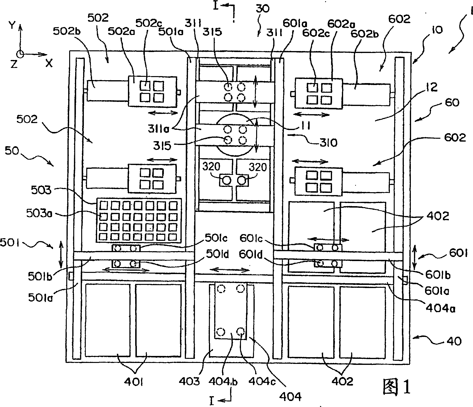
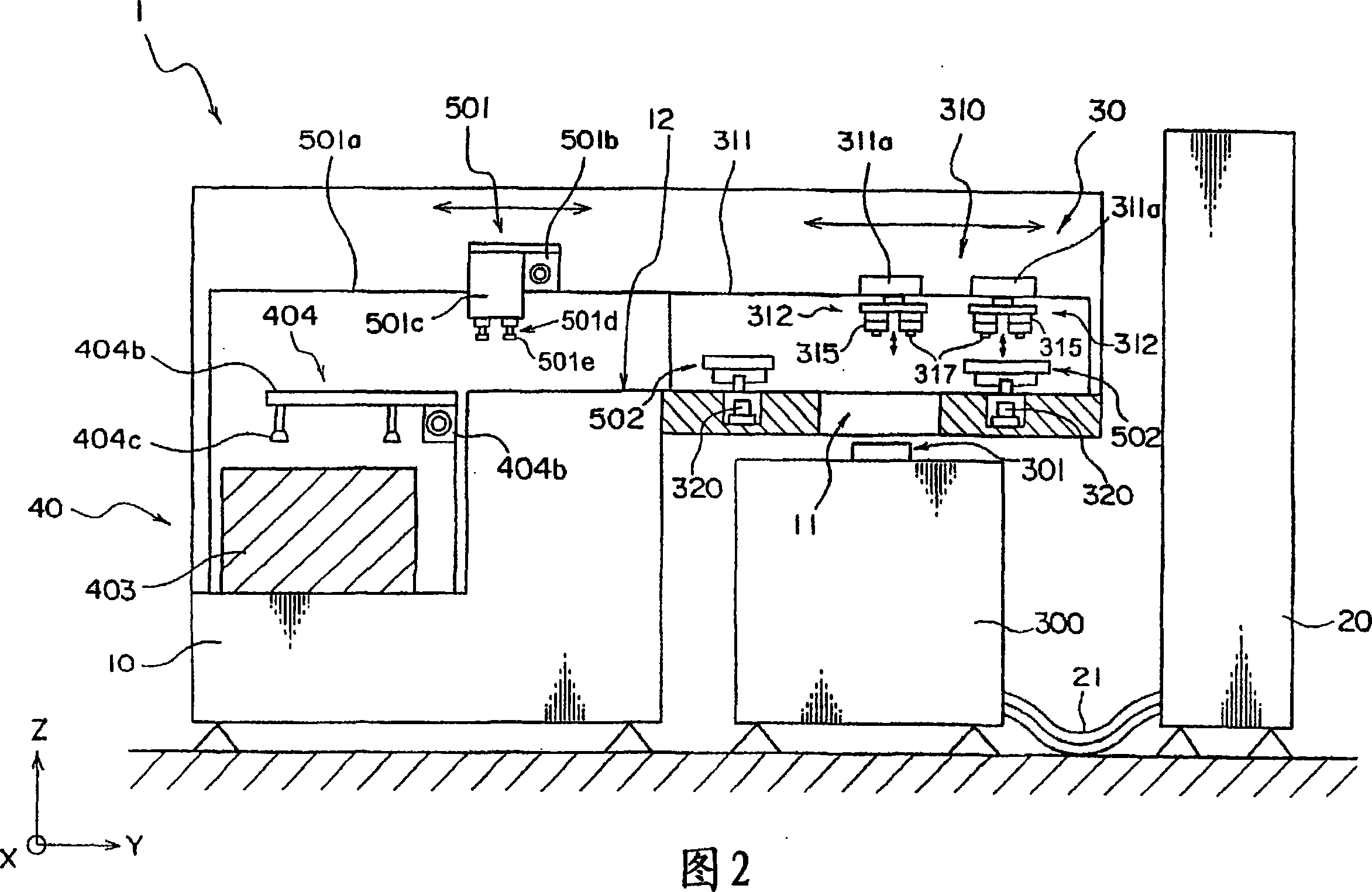
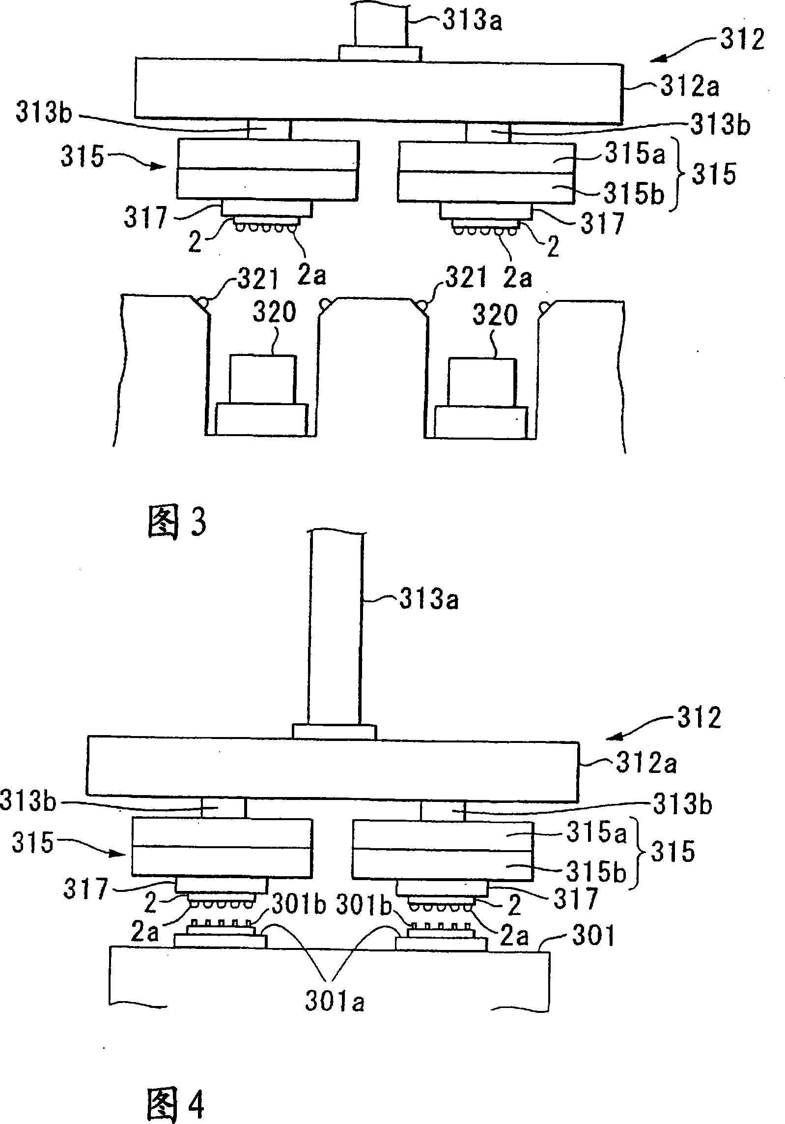
[0047] 1 is a plan view of a processing device according to an embodiment of the present invention; FIG. 2 is a sectional view (a sectional view along I-I in FIG. 1 ) viewed from a part of the processing device according to the same embodiment; FIG. 3 It is a view viewed from the side of the touch arm and the image capture device used in the processing device; FIG. 4 is a view viewed from the side of the touch arm and the contact part used in the processing device; FIG. 6 and 7 are schematic diagrams of the image processing steps in the processing device.

[0048] Note that the form of the IC device to be tested in this embodiment is, for example, a BGA or CSP (chip size package) with solder balls as device terminals, but the present invention is not limited thereto, and it may also be a device with pins as device terminals. QFP (small square planar package) or SOP (small out...


PUM


Abstract

Reference position information of each terminal of a reference electronic component is previously stored, an image of a terminal of an electronic component which is held by a carrying apparatus to be tested is picked up by an image pick-up apparatus, position information of each terminal is obtained from the image data of the terminal of the image-picked up electronic component to be tested, the reference position information of each terminal of the reference electronic component is compared with the obtained position information of each terminal of the electronic component to be tested, and lack and / or arrangement position failure of the terminal of the electronic component to be tested is judged.

Description

technical field [0001] The present invention relates to an electronic device processing device and a method for determining bad terminals, which can detect the absence or deviation of the arrangement positions of solder balls and pins of IC devices. Background technique [0002] In the manufacturing process of electronic devices such as IC devices, electronic device testing equipment is used to test the performance and function of the final manufactured electronic devices. [0003] As an example of the prior art, an electronic device testing apparatus is equipped with a test section for testing electronic devices, a loading section for sending pre-test IC devices to the test section, and a loading section for taking out post-test IC devices from the test section. IC devices and classify them in the unloading section. The loading section is provided with a buffer platform that can move back and forth between the loading section and the testing section, and is also provided w...

Claims


Application Information

Patent Timeline
Patent Type & Authority Applications(China)
IPC IPC(8): G01R31/26G01B11/00
CPCG01R31/2893H05K13/0413H05K13/0465G01R31/2891H05K13/04G01R31/26H01L22/00
Inventor 市川雅理
Owner ADVANTEST CORP
Why Eureka
Try Eureka