
Multi-line addressing methods and apparatus

An addressing and signaling technology, applied in the direction of cathode ray tube indicators, lighting devices, light sources, etc., can solve problems such as changes in the apparent brightness of pixels, and achieve reduced peak brightness, large color gamut, and reduced capacitive loss. Effect

Inactive Publication Date: 2007-11-07
CAMBRIDGE DISPLAY TECH LTD
View PDF17 Cites 3 Cited by
  • Summary
  • Abstract
  • Description
  • Claims
  • Application Information

AI Technical Summary

Problems solved by technology

In a conventional PWM scheme, the pixels are fully on or off, but due to integration within the viewer's eye, the apparent brightness of the pixel changes

Method used


Image

  • Multi-line addressing methods and apparatus
  • Multi-line addressing methods and apparatus
  • Multi-line addressing methods and apparatus

Examples


Embodiment Construction

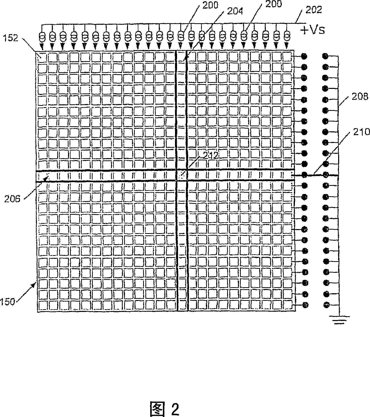
[0061] Consider a pair of rows of a passive matrix OLED display comprising a first row A and a second row B. In a conventional passive matrix driving scheme, the rows can be driven as shown in Table 1 below, with each row either fully on (1.0) or fully off (0.0).

[0062] A

B

open (1.0)

Off (0.0)

Off (0.0)

open (1.0)

[0063] Consider the ratio A / (A+B); in the example in Table 1 above, this ratio is either 0 or 1, but if neither row has pixels in the same column fully on, this ratio can be lowered and still provide the desired pixel brightness. In this way, the peak drive level can be reduced, extending the lifetime of the pixel.

[0064] In the first line scan, the brightness can be:

[0065] first cycle

[0066] 0.0 0.361 0.650 0.954 0.0

[0067] 0.0 0.015 0.027 0.039 0.0

[0068] second cycle

[0069] 0.2 0.139 0.050 0.046 0.0

[0070] 0.7 0.485 0.173 0.161 0.0

[0071] visible:

[0072] 1. In a single scan period, the r...


PUM


Abstract

This invention relates to methods and apparatus for driving emissive, in particular organic light emitting diodes (OLED) displays using multi-line addressing (MLA) techniques. Embodiments of the invention are particularly suitable for use with so-called passive matrix OLED displays. A method of driving an emissive display, the display comprising a plurality of pixels each addressable by a row electrode and a column electrode, the method comprising: driving a plurality of said column electrodes with a first set of column drive signals; and driving two or more of said row electrodes with a first set of forward bias row drive signals at the same time as said column electrode driving with said column drive signals; then driving said plurality of column electrodes with a second and subsequent sets of column drive signals; and driving said two or more row electrodes with a second and subsequent sets of forward bias row drive signals at the same time as said column electrode driving with said second column drive signals.

Description

technical field [0001] The present invention relates to methods and apparatus for driving emissive light emitting diode (Light Emitting Diode) displays, in particular Organic Light Emitting Diode (OLED) displays using Multi-Line Addressing (MLA) techniques. Embodiments of the invention are particularly suitable for use with so called passive matrix OLED displays. This application is one of three related applications sharing the same priority date. Background technique [0002] For example, multi-line addressing techniques for liquid crystal displays (LCDs) are described in US2004 / 150608, US2002 / 158832 and US2002 / 083655 to reduce the power consumption of LCDs and improve the relatively slow response rates of LCDs. However, since the fundamental difference between OLEDs and LCDs stems from the fact that the former is an emissive technology while the latter is a modulator form, the above technologies are not suitable for OLED displays. Furthermore, OLEDs provide a substantial...

Claims


Application Information

Patent Timeline
IPC IPC(8): G09G3/32G09G3/20G09G3/36G09G5/02
CPCG09G2310/04G09G5/02G09G2320/043G09G2300/0452G09G3/2014G09G2330/021G09G2310/06G09G2310/0208G09G2310/0297G09G3/3216G09G3/2022G09G3/20G09G3/30G09G3/32H05B33/12
Inventor 伊万·克里斯托弗·史密斯保罗·理查德·罗特利乔纳森·詹姆斯·M·霍尔斯
Owner CAMBRIDGE DISPLAY TECH LTD
Learn More