

Parallel bit test circuits for testing semiconductor memory devices and related methods
A technology for memory testing and testing circuits, applied in static memory, instruments, etc., which can solve the problems of prolonging the total test time of memory cells, increasing costs, and reducing productivity
- Summary
- Abstract
- Description
- Claims
- Application Information
AI Technical Summary
Problems solved by technology
Method used
Image

Examples
Embodiment Construction
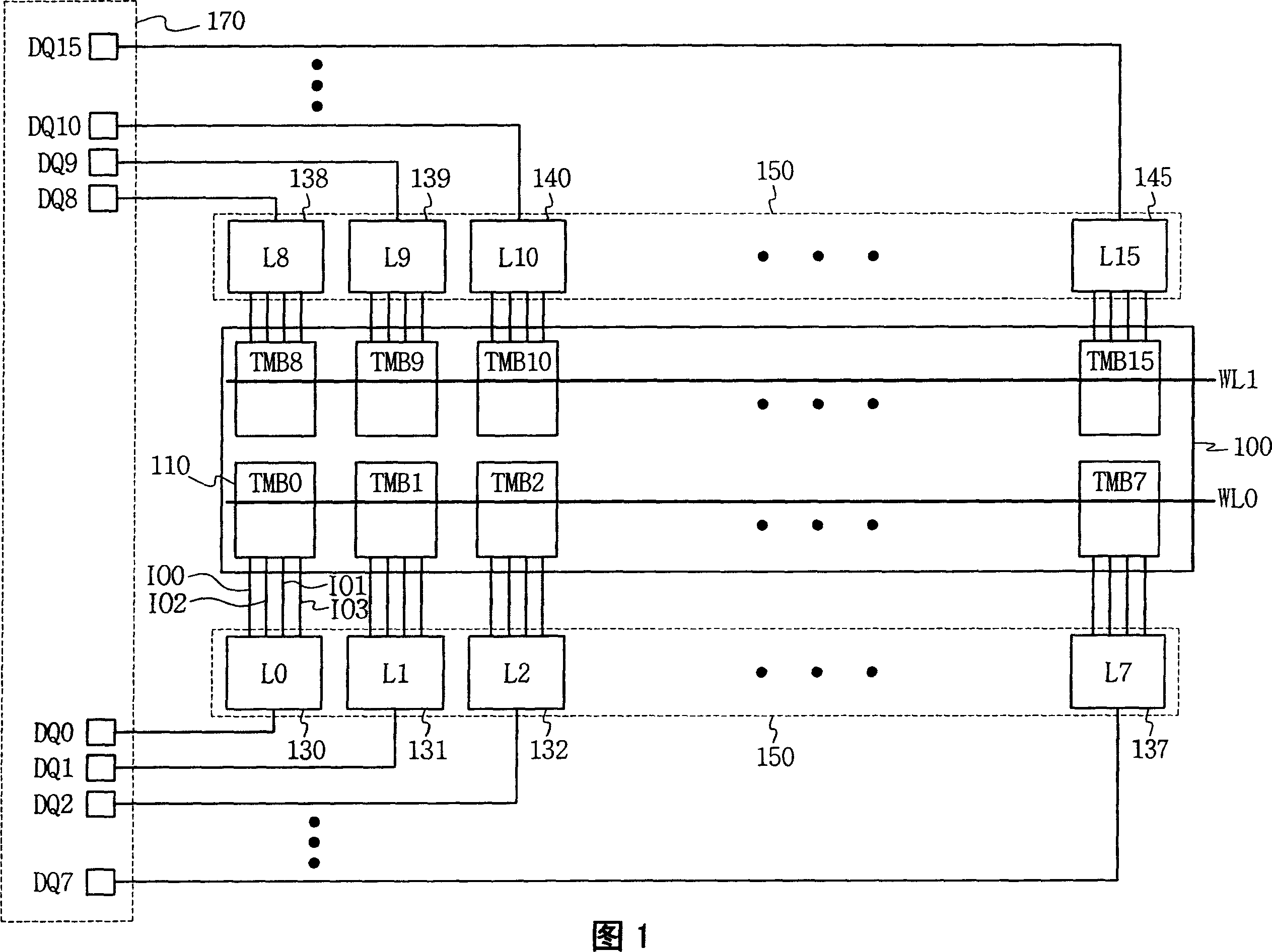
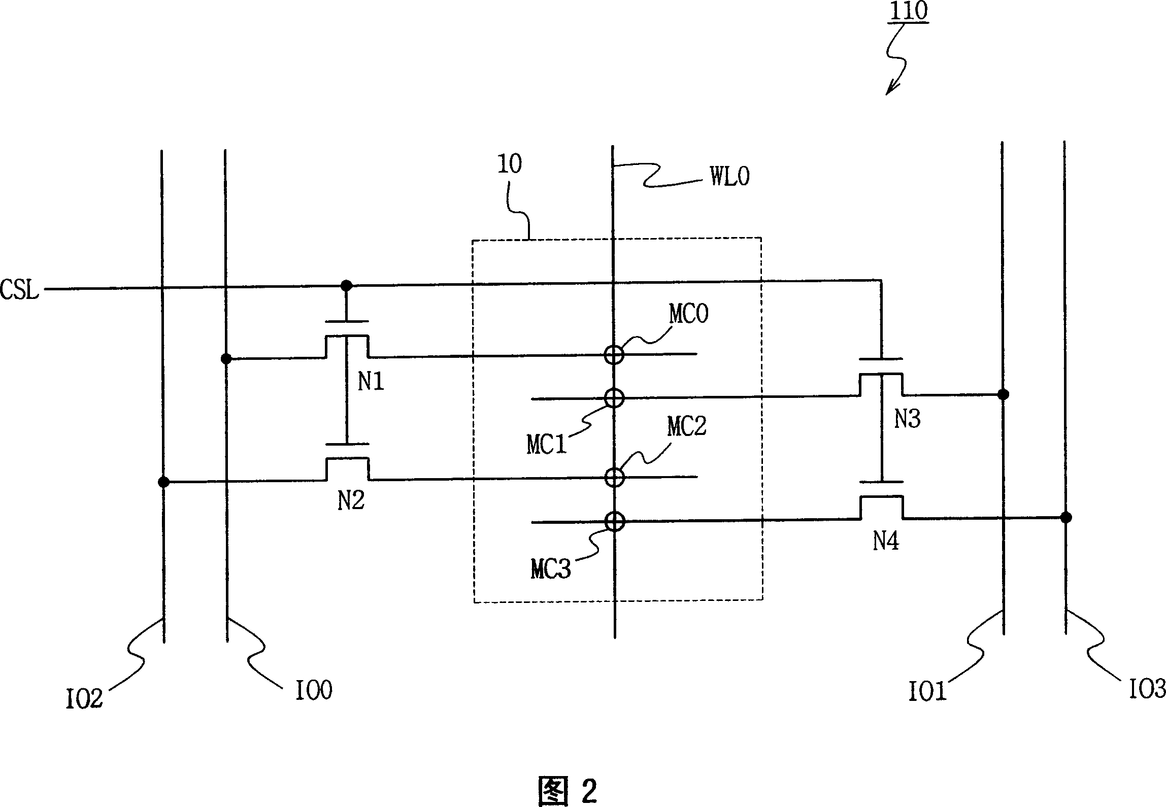
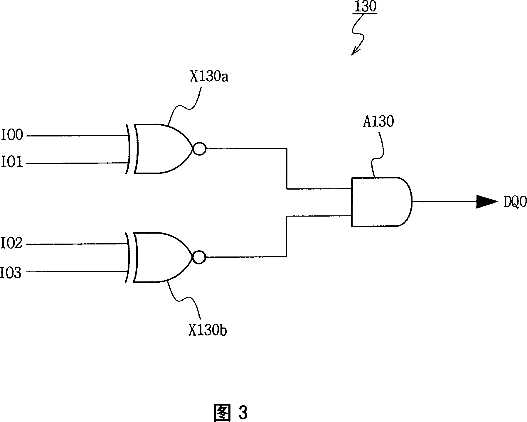
[0053] The present invention will be described more fully hereinafter with reference to the accompanying drawings, in which embodiments of the invention are shown. However, this invention may be embodied in many different forms and should not be construed as limited to the embodiments set forth herein. Rather, these embodiments are presented so that this disclosure will be thorough and complete, and will fully convey the scope of the invention to those skilled in the art. In the drawings, the size and relative sizes of elements and regions are exaggerated for clarity.
[0054] It will be understood that when an element or layer is referred to as being "on" or "connected to" another element or layer, it can be directly on the other element or layer, or directly connected to the other element or layer. connected, or intervening elements or layers may also be present. In contrast, when an element is referred to as being "directly on" or "directly connected to" another element o...
PUM
 Abstract
Description
Claims
Application Information