Random access memory having test circuit

A technology for testing circuits and memory, applied in static memory, instruments, etc., can solve problems such as low data volume

Inactive Publication Date: 2007-11-28
QIMONDA
View PDF0 Cites 7 Cited by
  • Summary
  • Abstract
  • Description
  • Claims
  • Application Information

AI Technical Summary

Problems solved by technology

Using this method, the amount of data read from the storage device at a given time will b

Method used


Image

  • Random access memory having test circuit
  • Random access memory having test circuit
  • Random access memory having test circuit

Examples


Embodiment Construction

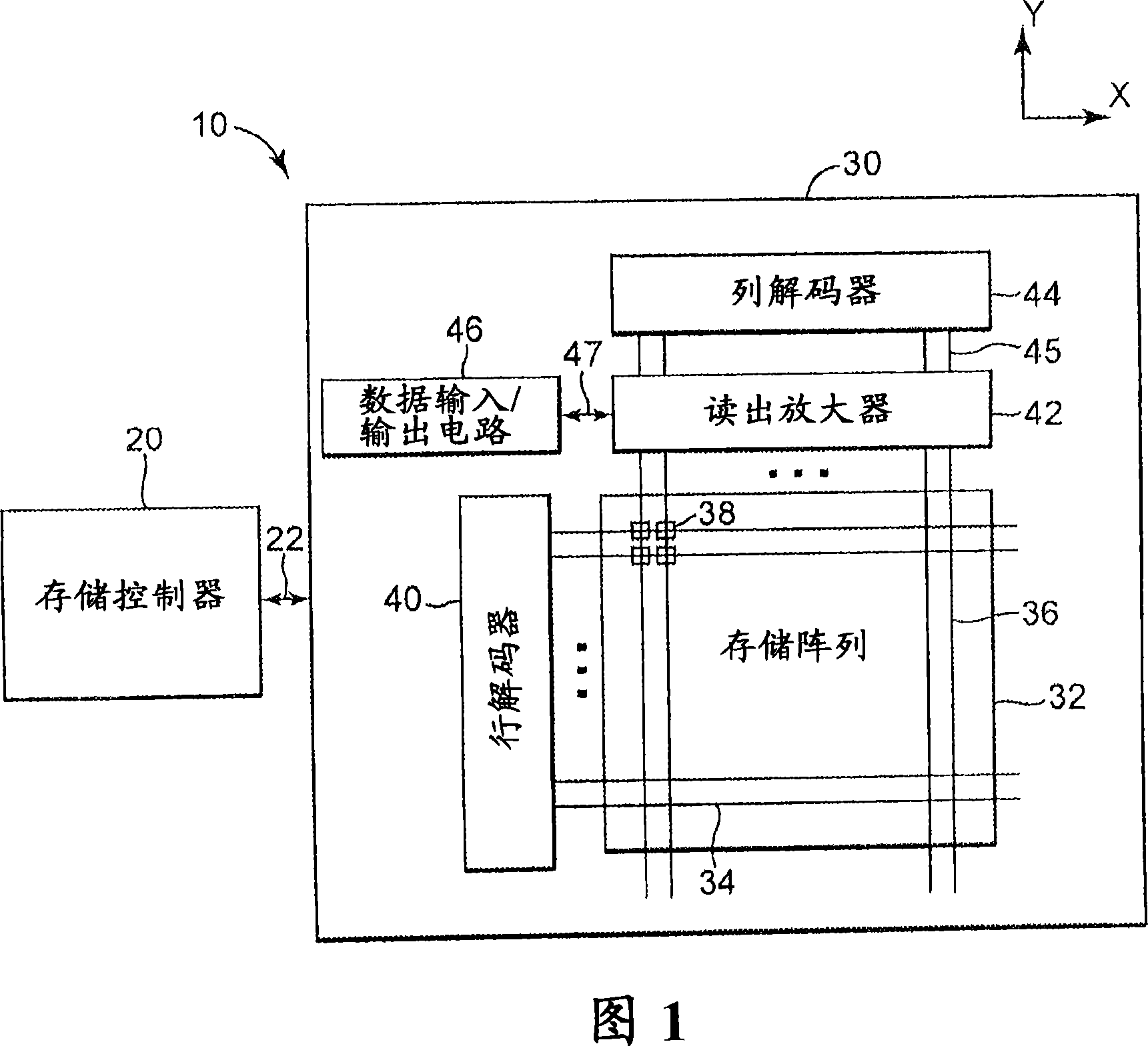
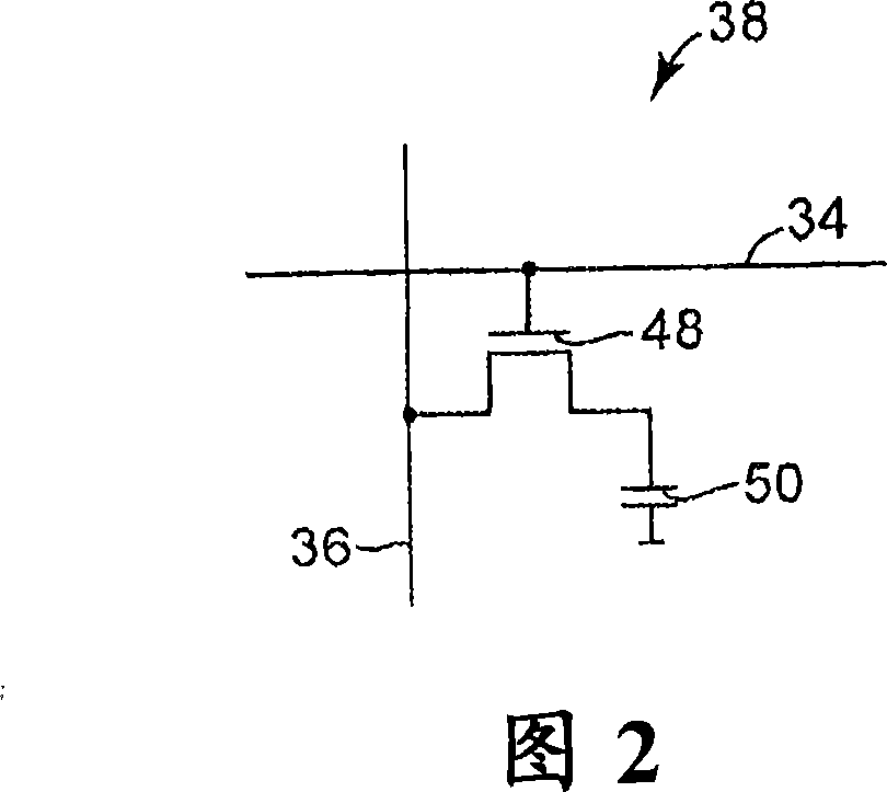
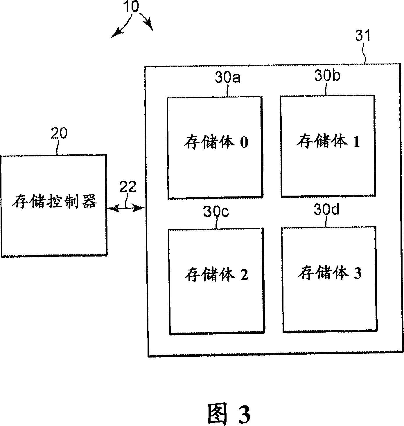
[0011] FIG. 1 is a block diagram illustrating an embodiment of a memory 10 . In this embodiment, memory 10 is a random access memory such as dynamic random access memory (DRAM), synchronous dynamic random access memory (SDRAM), double data rate synchronous dynamic random access memory (DDR SDRAM), dual data rate rate two synchronous dynamic random access memory (DDR2SDRAM), pseudo static random access memory (PSRAM), magnetic random access memory (MRAM), or flash memory. The memory 10 includes a memory controller 20 and at least one memory bank 30 . The memory bank 30 includes a memory cell array 32 , a row decoder 40 , a column decoder 44 , a sense amplifier 42 and a data input / output circuit 46 . Memory controller 20 is electrically connected to memory bank 30 by communication link 22 .

[0012] The memory 10 includes a normal operation mode and a backend test mode. The memory 10 is configured to perform back-end testing in a back-end test mode that tests the memory 10 af...


PUM


Abstract

A memory circuit comprises a memory and a first test circuit coupled to the memory. The first test circuit is configured to compare data read from memory cells with expected data for the memory cells to provide a first set of pass/fail signals for the memory cells, compress the first set of pass/fail signals for the memory cells into a second pass/fail signal, latch the second pass/fail signal in response to a data valid signal, maintain the latch of the second pass/fail signal if the second pass/fail signal indicates a failed test, combine the second pass/fail signal and a third pass/fail signal of a second test circuit to provide a fourth pass/fail signal, and pass the fourth pass/fail signal to a third test circuit.

Description

Background technique [0001] After wafer processing, there are usually two main testing phases in the DRAM manufacturing process. The first major test phase consists of front-end testing, also known as wafer testing, which tests the silicon wafer as a whole by touching the individual chips on the wafer with probe cards. During this manufacturing stage, it is usually determined whether a defect in the storage area can be repaired by a fuse link. The second main testing phase is back-end testing, also known as module testing, which is performed after the packaged chip or module has been repaired if necessary. During this manufacturing stage, further repairs on individual chips are generally not possible. Thus, the tests performed may differ from the front-end tests, and thus the location and number of faults, if any, are not required, or are required for statistical purposes only. [0002] Many efforts have been made in the manufacturing industry to reduce the costly test time...

Claims


Application Information

Patent Timeline
IPC IPC(8): G11C29/00
CPCG11C29/40
Inventor W·霍肯梅尔
Owner QIMONDA
Why Eureka
Try Eureka