

Method for producing air bridge of compound semiconductor microwave high power device
A technology of high-power devices and manufacturing methods, applied in the field of microelectronics, can solve the problems of small protrusion in the vertical vertical plane, increase the thickness of the photoresist, and shrink the photoresist laterally, so as to ensure reliability, reduce difficulty, and arch large arc effect
- Summary
- Abstract
- Description
- Claims
- Application Information
AI Technical Summary
Benefits of technology
Problems solved by technology
Method used
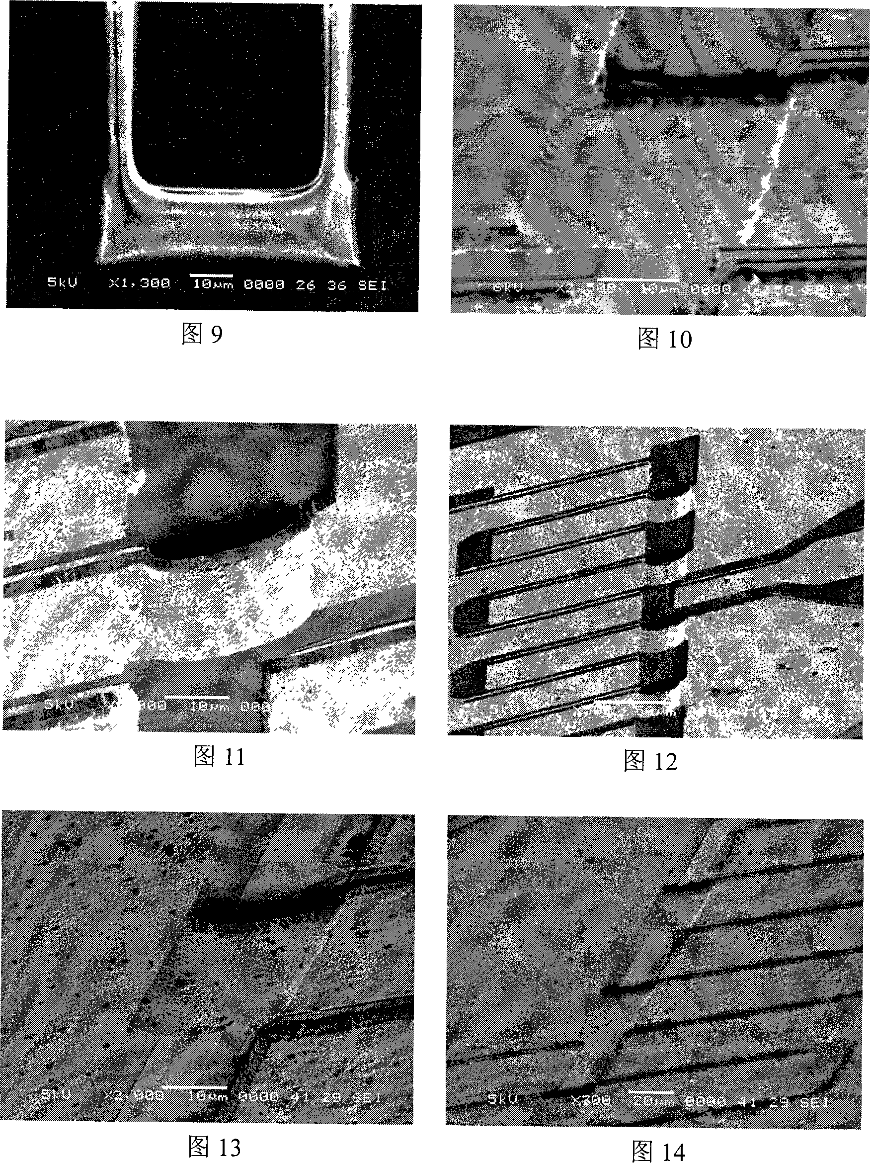
Image

Examples
Embodiment 1
[0057] The substrate material chooses Si wafer as the substrate
[0058] In step 1, two kinds of adhesives are respectively coated on the Si substrate, and a bridge region and an electrode region are photoetched to form a sacrificial layer.
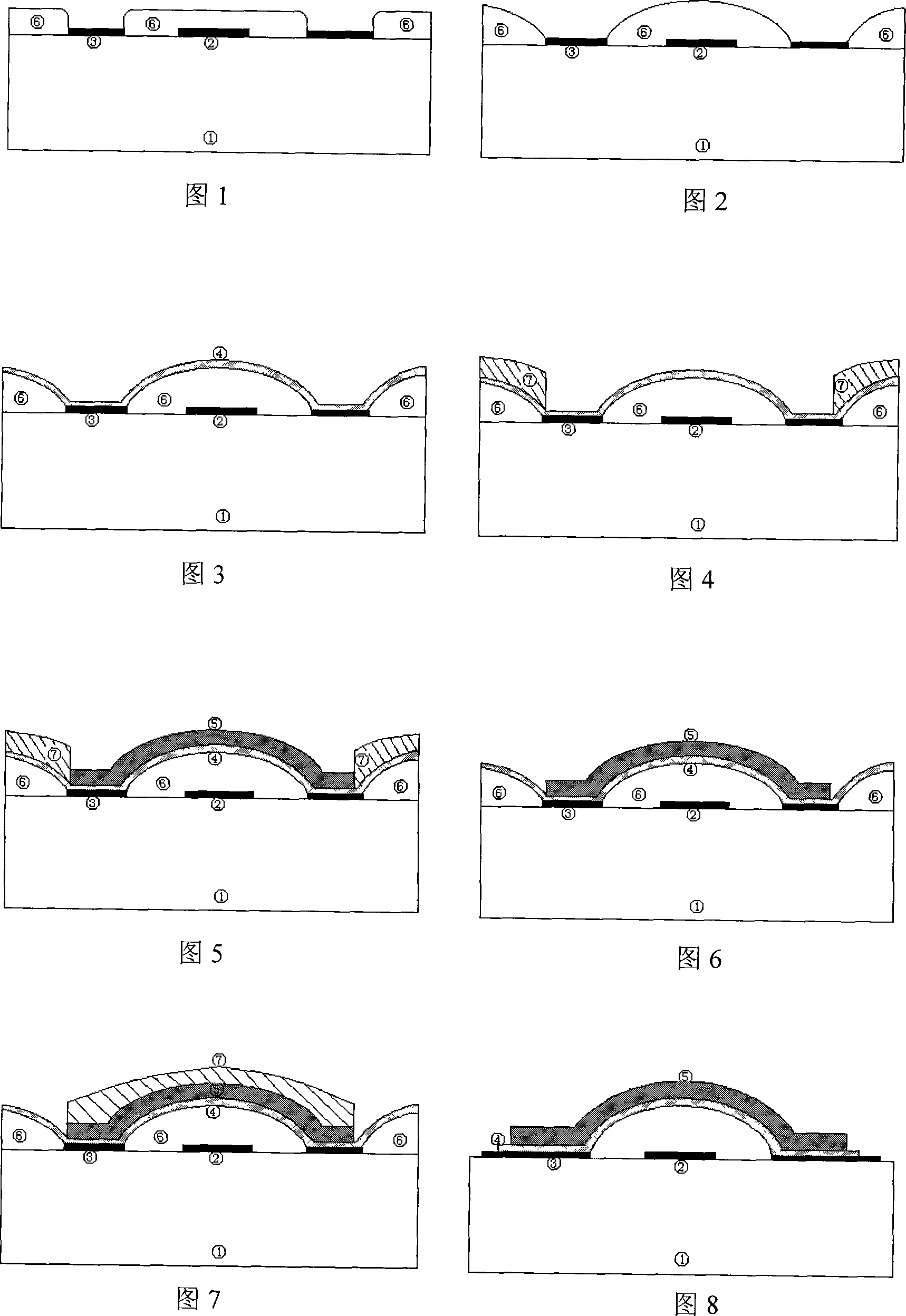
[0059] First, coat a layer of 1.5 μm thick peeling adhesive LOR5A on the Si substrate, bake in an oven at a temperature of 160°C for 20 minutes; then coat a layer of 1.5 μm thick photoresist EPI622, and bake at a temperature of 85°C for 10 minutes. The ratio of the stripping glue LOR5A and the photoresist EPI622 is 5:5; then use the first photolithography plate to make the air bridge to lithography the area of the bridge, the bridge pier, that is, the electrode, and finally soak in the developer for 2 minutes, and blow dry with nitrogen , forming a 3 μm sacrificial layer, as shown in Figure 1.
[0060] Step 2, low-temperature baking, so that the sacrificial layer in the bridge area forms an arched structure.
[0061] Bake the substrat...
Embodiment 2
[0079] The invention manufactures the air bridge device structure on the microwave high-power GaN HEMT substrate based on the source, drain contact and Schottky contact, that is, the air bridge device structure on the microwave high-power gallium nitride high electron mobility transistor substrate .
[0080] In step 1, two kinds of adhesives are respectively coated on the GaN substrate, and the bridge region and the electrode region are photoetched to form a sacrificial layer.
[0081] Firstly, coat a layer of 1.5μm thick stripping adhesive LOR5A on the GaN substrate, and bake it in an oven at 160°C for 20min; then coat a layer of 2.0μm thick photoresist EPI622, and bake it at 85°C for 10min , the ratio of the stripper LOR5A to the photoresist EPI622 is 3:4;
[0082] Then use the first photolithography plate for making the air bridge to lithographically cut out the area of the bridge, pier, or electrode, and finally soak in the developer solution for 2 minutes, and blow dry...
Embodiment 3
[0102] The substrate material is GaN as the substrate.
[0103] In step 1, two kinds of adhesives are respectively coated on the GaN substrate, and the bridge region and the electrode region are photoetched to form a sacrificial layer.
[0104]First, coat a layer of 1.0 μm thick peeling adhesive LOR5A on the GaN substrate, and bake it in an oven at a temperature of 160°C for 20 minutes; then coat a layer of 1.5 μm thick photoresist EPI622, and bake it at a temperature of 85°C for 10 minutes. The ratio of stripping glue LOR5A and photoresist EPI622 is 2:3; then use the first photolithography plate for making air bridges to photoetch out the area of bridges, piers, or electrodes, and finally soak in the developer for 2 minutes, and blow dry with nitrogen , forming a 2.5 μm sacrificial layer, as shown in Figure 1.
[0105] Step 2, low-temperature baking, so that the sacrificial layer in the bridge area forms an arched structure.
[0106] Bake the substrate on which the sacrif...
PUM
| Property | Measurement | Unit |
|---|---|---|
| Thickness | aaaaa | aaaaa |
| Thickness | aaaaa | aaaaa |
| Thickness | aaaaa | aaaaa |
Abstract
Description
Claims
Application Information