
Semiconductor memory, controller and method for operating semiconductor memory

一种存储器、半导体的技术,应用在静态存储器、数字存储器信息、信息存储等方向

Inactive Publication Date: 2008-01-16
SOCIONEXT INC
View PDF1 Cites 13 Cited by
  • Summary
  • Abstract
  • Description
  • Claims
  • Application Information

AI Technical Summary

Problems solved by technology

A technique that can mask data without increasing the number of external terminals when the number of data bytes increases and the number of bits of the data masking signal increases

Method used


Image

  • Semiconductor memory, controller and method for operating semiconductor memory
  • Semiconductor memory, controller and method for operating semiconductor memory
  • Semiconductor memory, controller and method for operating semiconductor memory

Examples


Embodiment Construction

[0022] Embodiments of the present invention will be described below with reference to the drawings. A signal line shown as a thick line in the figure is composed of a plurality of lines. Also, some blocks to which thick lines are connected are constituted by a plurality of circuits. The same symbol as the signal name is used for the signal line that carries that signal. Signals beginning with " / " indicate negative logic. Double circles in the figure indicate external terminals.

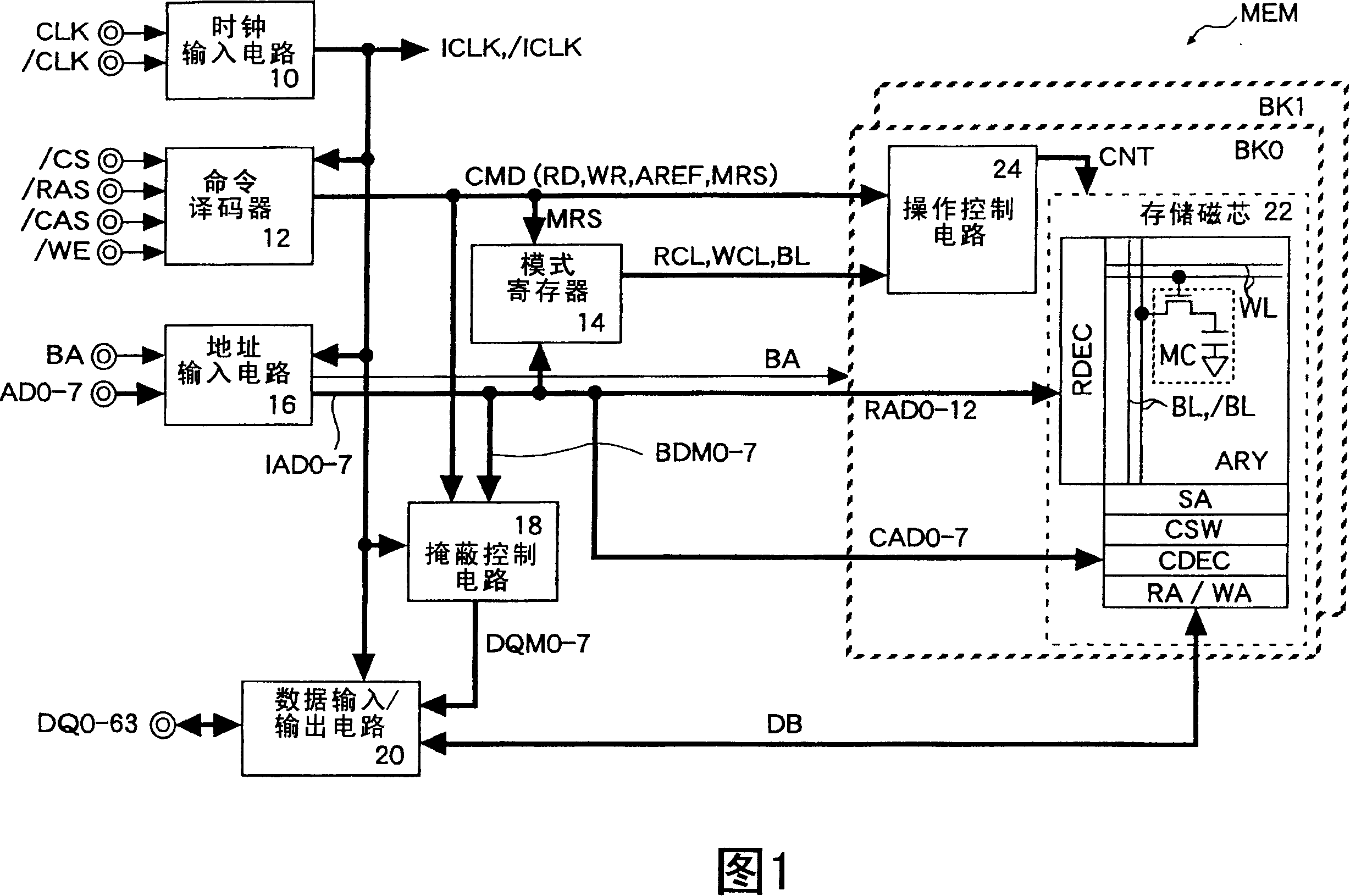
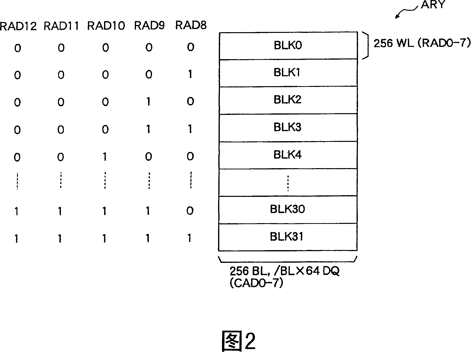
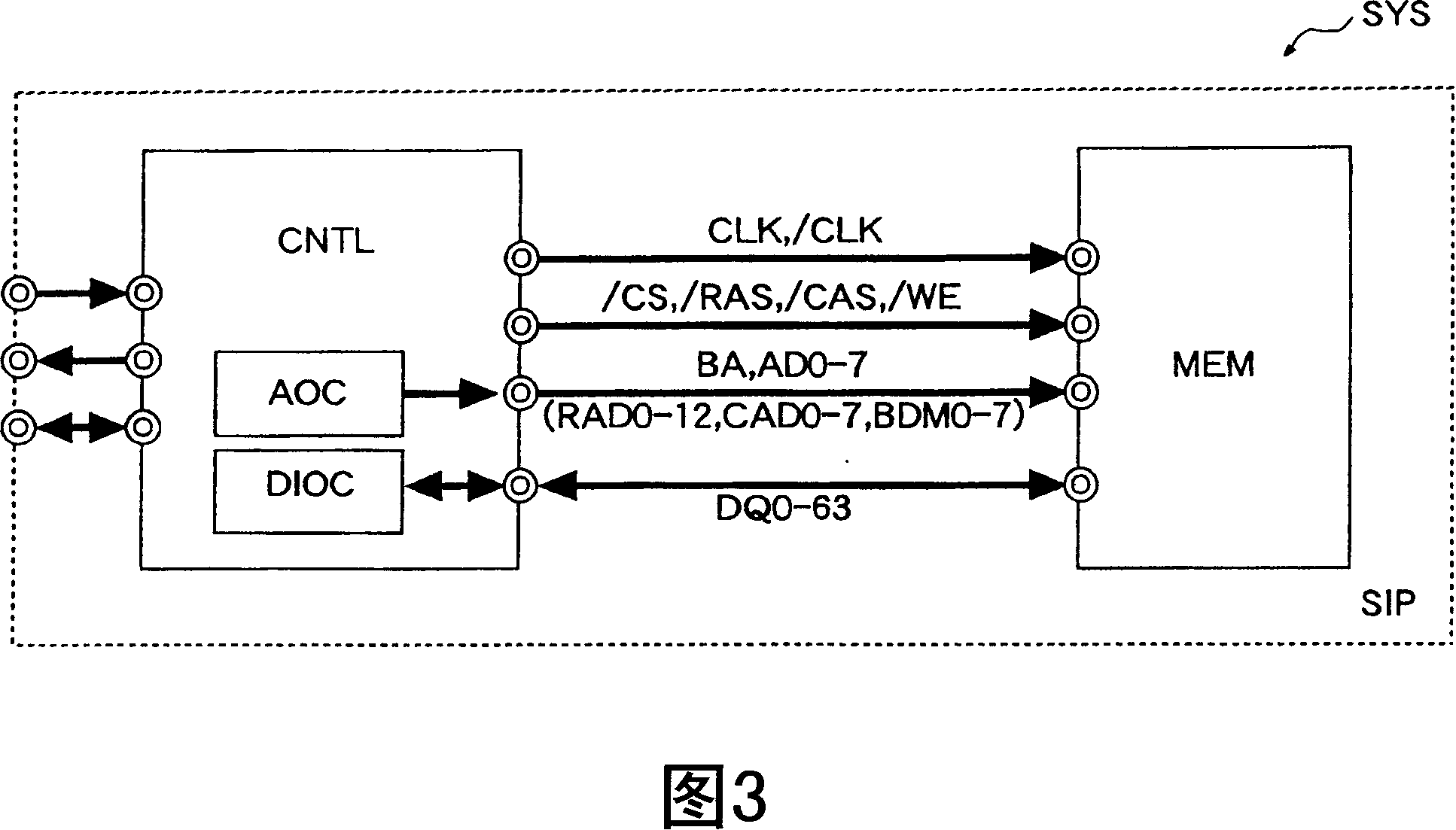
[0023] FIG. 1 is a block diagram showing a first embodiment of the present invention. The semiconductor memory MEM is, for example, a clock synchronous type FCRAM (Fast Cycle RAM) that operates in synchronization with an external clock CLK. FCRAM is a pseudo-SRAM having a memory cell of DRAM and an interface of SDRAM. The memory MEM includes a clock input circuit 10, a command decoder 12, a mode register 14, an address input circuit 16, a mask control circuit 18, a data input / output circuit 20, a...


PUM


Abstract

To perform mask control of data signals without increasing the number of external terminals even when the number of bits in a data mask signal is large, an address input circuit sequentially receives a first address signal, a second address signal, and a first data mask signal supplied to an address terminal in synchronization with transition edges of a clock signal. Namely, the first data mask signal is supplied to the address terminal at a different timing from timing at which the first and second address signals are received. The first address signal, second address signal, and first data mask signal are output, for example, from a controller accessing a semiconductor memory. A data input / output circuit inputs / outputs data via a data terminal and masks at least either of write data to memory cells and read data from the memory cells in accordance with logic of the first data mask signal.

Description

technical field [0001] The present invention relates to a semiconductor memory and a controller for accessing the semiconductor memory. Background technique [0002] With the advancement of semiconductor manufacturing technology, the number of components that can be mounted in a controller such as an ASIC (Application Specific IC) is also increasing year by year. In response to the increase in the number of components, it has become possible to mount various functional block chips on a single ASIC, which were conventionally configured with separate chips. As ASICs have higher-level features, the number of external terminals tends to increase. Furthermore, in order to increase the data transfer rate, the number of data terminals tends to increase. Since the size of a pad as an external terminal is determined based on packaging technology, the pad size cannot be reduced at the same rate as the component size even when the component size is reduced with the advancement of sem...

Claims


Application Information

Patent Timeline
Patent Type & Authority Applications(China)
IPC IPC(8): G11C11/34G11C7/10G11C8/04G11C29/24G11C7/22
CPCG11C7/1066G11C7/1093G11C7/1045G11C11/4096G11C11/4094G11C7/1006G11C7/12G11C7/1078G11C7/22G11C7/1051G11C11/4076G11C11/4093G11C11/408
Inventor 神田达哉佐藤光德
Owner SOCIONEXT INC
Learn More