Encapsulation structure for preventing adhesive crystal glue from polluting wafer welding cushion
A chip and die bonding technology, applied in the field of semiconductor packaging, can solve the problems of not being able to use high-density COB packaging, polluting pads 122, and polluting wire bonding fingers, etc.
- Summary
- Abstract
- Description
- Claims
- Application Information
AI Technical Summary
Problems solved by technology
Method used
Image
Examples
no. 1 Embodiment
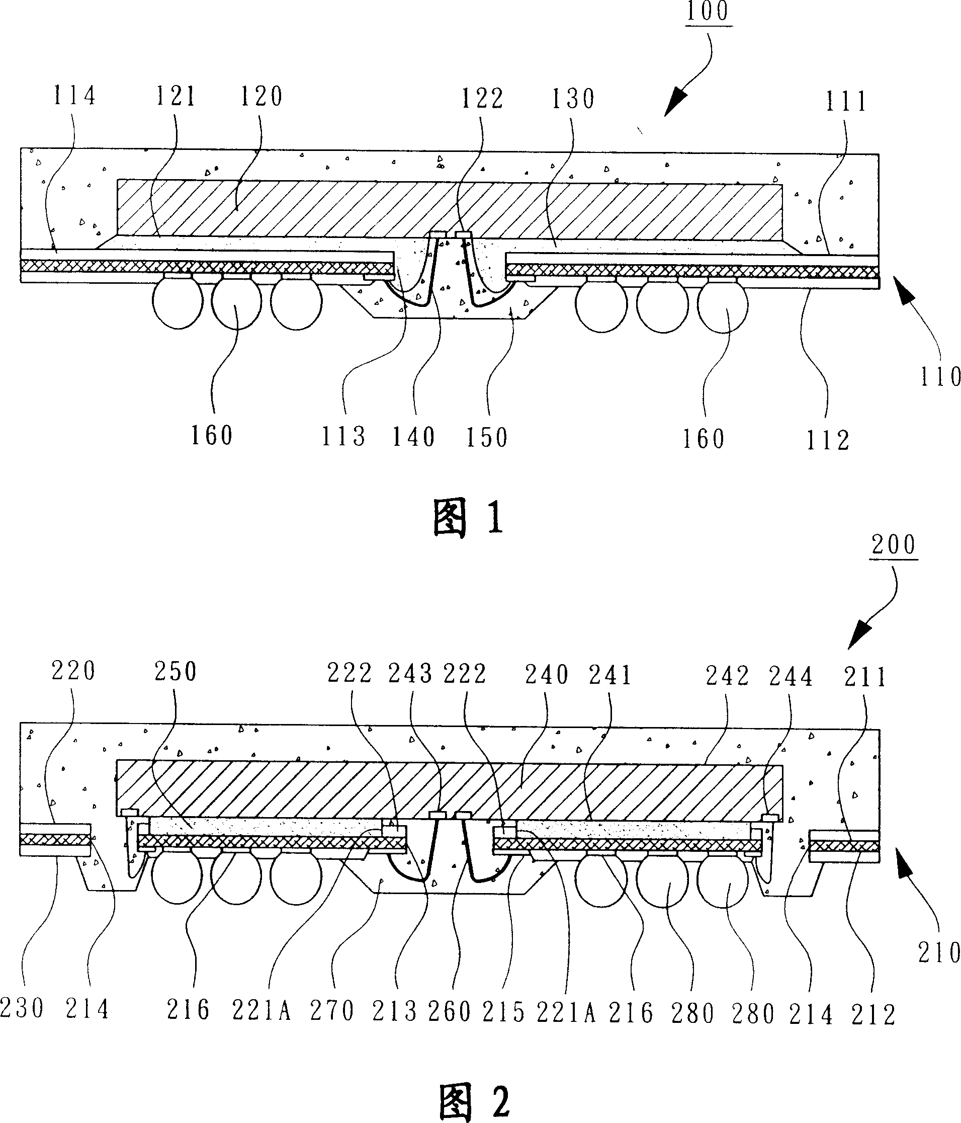
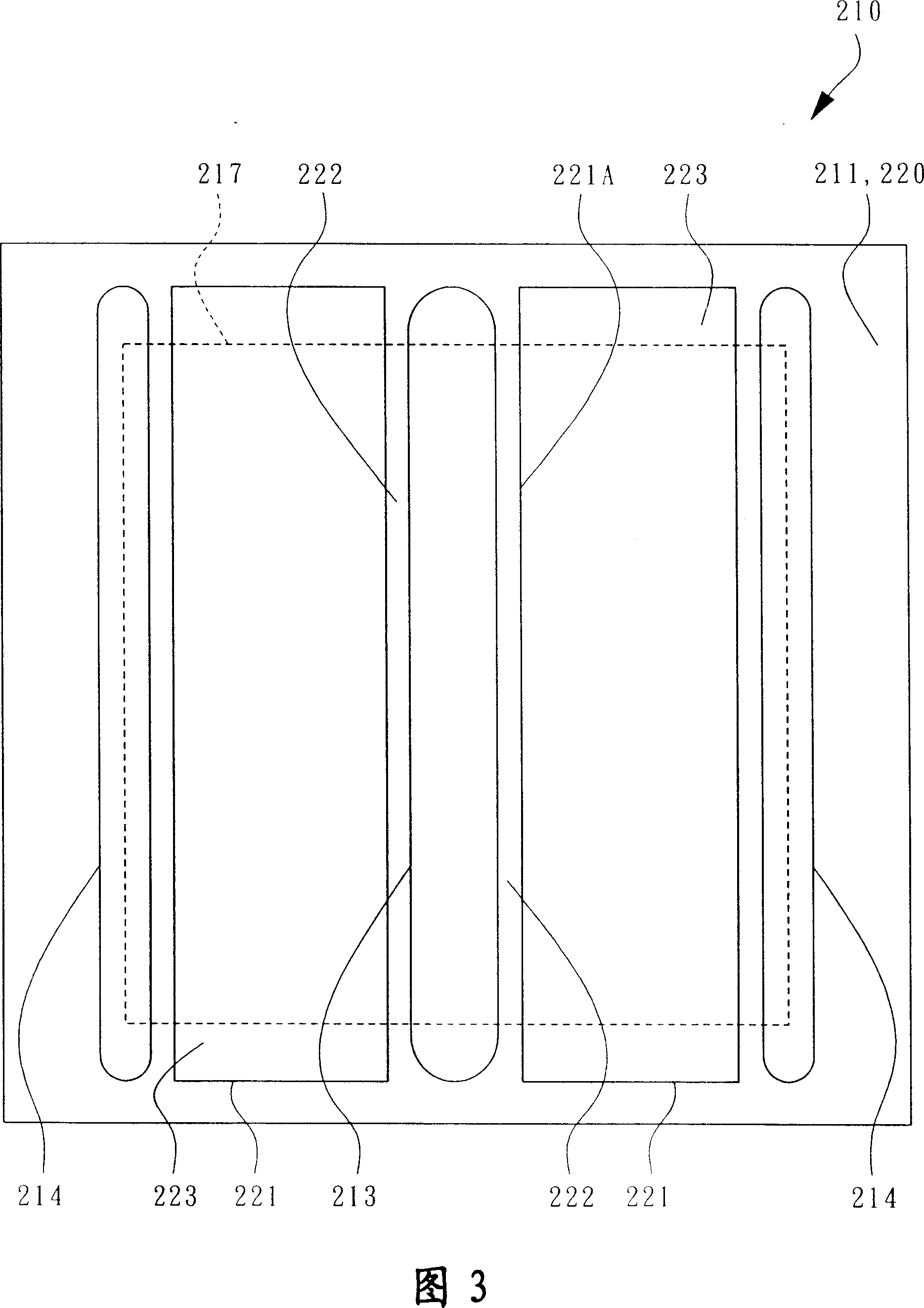
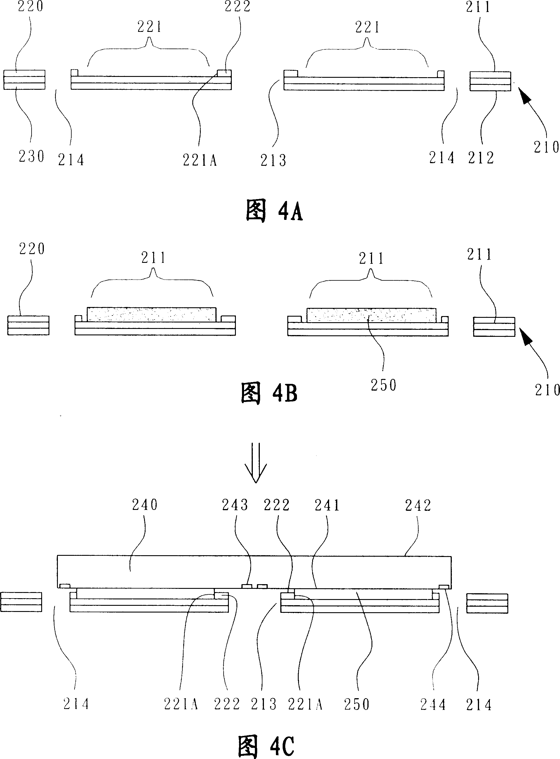
[0076] According to the first specific embodiment of the present invention, FIG. 2 is a schematic cross-sectional view of a package structure for preventing die bonding glue from contaminating chip pads. FIG. 3 is a schematic view of the upper surface of the substrate used in the package structure. FIGS. 4A to 4C are Schematic cross-sectional view of the substrate during the die-bonding process.
[0077] As shown in FIG. 2 , a packaging structure 200 of the present invention for preventing die bonding glue from contaminating chip pads mainly includes a substrate 210 , a chip 240 , a die bonding glue 250 , a plurality of bonding wires 260 and an encapsulant 270 . Generally, the substrate 210 can be a printed circuit board, which has an upper surface 211, a lower surface 212, and a plurality of wiring channels 213, 214, wherein the wiring channels 213, 214 can be elongated slots, and run through the The upper surface 211 and the lower surface 212 are used for the bonding wires 2...
PUM
 Abstract
Description
Claims
Application Information


