Wafer container with secondary wafer restraint system

A wafer and container technology, applied in the field of wafer confinement system, can solve problems such as damaged wafers, wafer cross slots, wafer movement, etc.

Inactive Publication Date: 2008-02-06
ENTEGRIS INC
View PDF7 Cites 5 Cited by
  • Summary
  • Abstract
  • Description
  • Claims
  • Application Information

AI Technical Summary

Problems solved by technology

However, prior art wafer confinement structures are not very satisfactory in some situations
In some cases, the wafer confinement structure may allow the wafer to translate too far vertically during a physical shock event, cau

Method used


Image

  • Wafer container with secondary wafer restraint system
  • Wafer container with secondary wafer restraint system
  • Wafer container with secondary wafer restraint system

Examples


Embodiment Construction

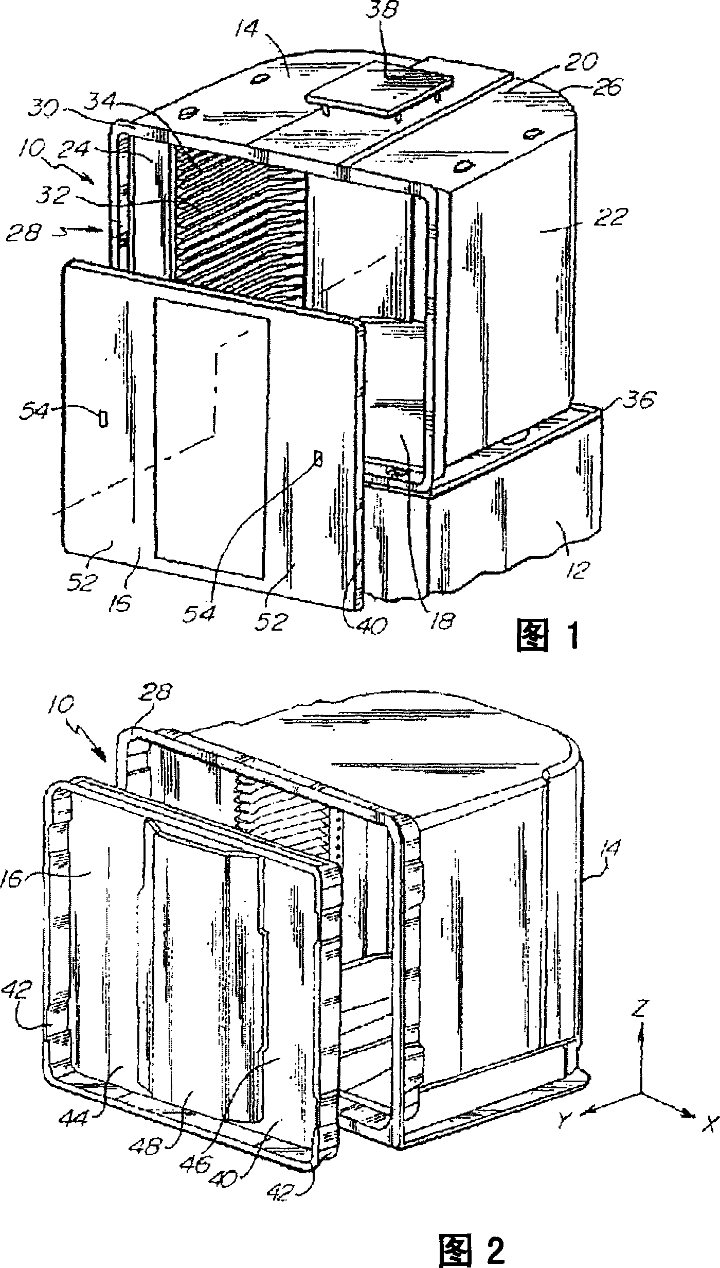
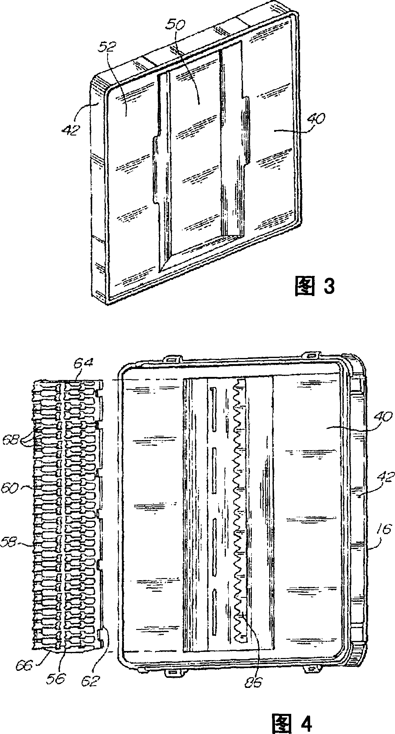
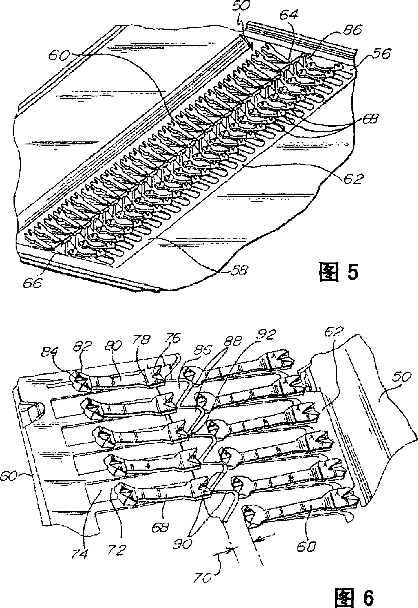
[0058] A wafer container 10 according to the present invention is shown in FIG. 1 on a processing tool 12 . Wafer container 10 generally includes an enclosure 14 and a door 16 . Housing 14 is generally made of polycarbonate or other suitable thermoplastic material and includes a bottom 18 , a top 20 , opposing sides 22 , 24 , and a back 26 . Opposite the back 26 is an open front 28 defined by a door frame 30 . One or more wafer support structures 32 with a plurality of wafer support frames 34 are positioned within the housing 14 for receiving a plurality of semiconductor wafers or substrates spaced apart in a generally parallel, axially aligned arrangement. (not shown). A power coupling 36 and a robotic handling flange 38 may be positioned on the outer surfaces of the bottom 18 and top 20, respectively, to enable automatic handling equipment to transfer and use the containers. Detailed descriptions of the construction and use of wafer containers and support members are disc...


PUM


Abstract

A wafer container providing improved wafer restraint during physical shock events. In embodiments of the invention, a secondary wafer restraint structure defining a plurality of notches is interposed between opposing wafer restraint members on the door of the container. The notches may be defined by one or more converging edges or surfaces meeting at a junction. The junctions are positioned so as to align with the wafer receiving portions of each opposing pair of wafer restraint member so that when the door is fully sealingly engaged with the enclosure of the container, the edge of the wafer is contacting the junction. In this position, any vertical movement of the wafer due to shock imparted to the container causes the wafer to contact the converging surfaces or edges, thereby limiting such movement. The positioning of the secondary wafer restraint structure between and proximate opposing fingers of the primary wafer restraint limits deflection of the wafer between support points and thereby further inhibits the wafer from ''jumping'' out of the supports and cross-slotting.

Description

[0001] Related applications [0002] This application claims rights based on U.S. Provisional Patent Application No. 60 / 630,546, filed November 23, 2004, and entitled "Wafer Container With Auxiliary Wafer Confinement System ( WAFER CONTAINER WITH SECONDARY WAFERRESTRAINT SYSTEM), which is hereby incorporated by reference in its entirety. technical field [0003] The present invention relates generally to sealable containers for semiconductor wafers, and more particularly to wafer containment systems for wafer containers. Background technique [0004] Converting semiconductor wafers into integrated circuit chips often involves many steps in which the wafers are repeatedly handled, stored and shipped. Wafers must be transported between workstations and between fabs. Wafers are fragile and easily damaged by physical shock. Additionally, electrostatic charge buildup and discharge near semiconductor wafers can cause severe damage. Due to the damage-prone nature and high value...

Claims


Application Information

Patent Timeline
IPC IPC(8): B65D85/48
Inventor 约翰·布恩斯马修·A·伏勒杰弗瑞·J·金马丁·L·福柏斯马克·V·斯密斯
Owner ENTEGRIS INC
Why Eureka
Try Eureka