SiC MOSFET sub-module unit and crimping type package thereof

A crimp-type, sub-mold technology, applied in electrical components, semiconductor/solid-state device parts, semiconductor devices, etc., can solve the problem that silicon carbide devices are difficult to be crimped and packaged.

Pending Publication Date: 2021-09-10
XI AN JIAOTONG UNIV
View PDF0 Cites 2 Cited by
  • Summary
  • Abstract
  • Description
  • Claims
  • Application Information

AI Technical Summary

Problems solved by technology

[0008] The purpose of the present invention is to provide a SiC MOSFET sub-module unit and its crimp-type packaging to overcome the problem that silicon carbide devices are difficult to carry out crimp-type packaging

Method used


Image

  • SiC MOSFET sub-module unit and crimping type package thereof
  • SiC MOSFET sub-module unit and crimping type package thereof
  • SiC MOSFET sub-module unit and crimping type package thereof

Examples


Embodiment Construction

[0040] Embodiments of the present invention are described in further detail below:

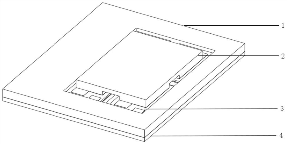
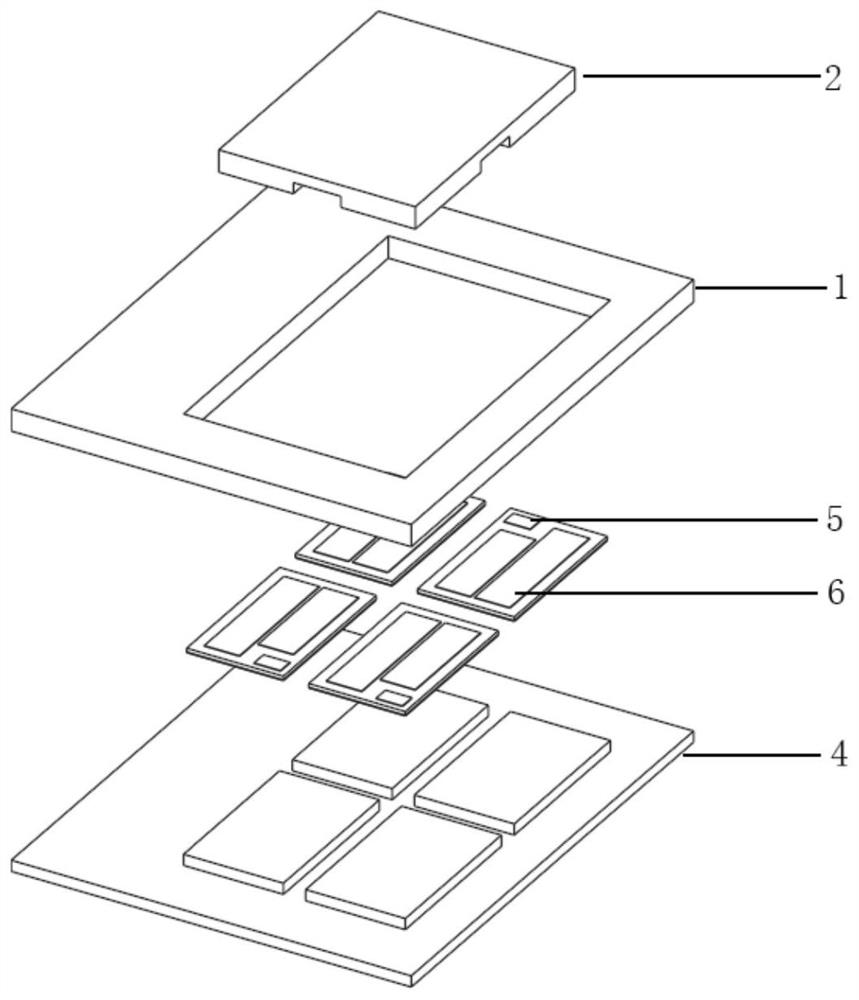
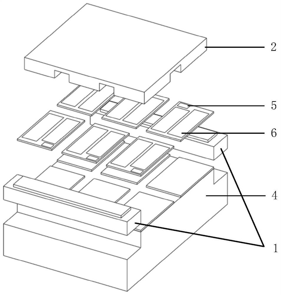
[0041] The SiCMOSFET sub-module unit designed in the present invention includes a source molybdenum sheet 2 , a SiCMOSFET chip array 3 , a DBC ceramic substrate 1 and a drain molybdenum sheet 4 . The lower surface of the source molybdenum sheet 2 is cut into four raised areas, and each raised area is respectively connected to the source 6 of the SiCMOSFET chip array 3 through nano-silver sintering, and does not cover the gate and terminal ; The SiCMOSFET chip array 3, each sub-module contains four pieces, one side of the source 6 faces upwards, and the grid 5 faces the outside, and is connected to the DBC ceramic substrate 1 on its periphery through bonding wires; the drain Pole molybdenum sheet 4, one side of which is connected to the drain of the SiCMOSFET chip array 3 through nano-silver sintering; The edge is a smooth arc; the internal gap of the SiCMOSFET sub-module unit 9 is filled with...


PUM


Abstract

The invention discloses a SiC MOSFET sub-module unit and crimping type packaging thereof, belongs to the technical field of semiconductor device packaging, and solves the problem that an existing SiC power chip is difficult to crimp and package. Each SiC MOSFET sub-module unit comprises a DBC (Direct Bond Copper) ceramic substrate, a source electrode molybdenum sheet, a SiCMOSFET chip array and a drain electrode molybdenum sheet; and N SiCMOSFET chips are arranged on the upper surface of the source electrode molybdenum sheet, N first protrusions are symmetrically arranged on the lower surface of the source electrode molybdenum sheet, the first protrusions are connected with the N SiCMOSFET chips respectively, grid electrodes and source electrodes of the SiCMOSFET chips are exposed, N second protrusions used for connecting and positioning the SiCMOSFET chips are arranged on the upper surface of the drain electrode molybdenum sheet, the SiCMOSFET chip array is composed of the N SiCMOSFET chips, and the exposed grid electrodes and source electrodes of the SiCMOSFET chips are connected to the DBC ceramic substrate. The power density of the module is improved, the heat dissipation capability is enhanced, the reliability of the device is improved, the insulation level of the module is improved by filling the module with silica gel, and the module can be applied to the high-voltage field.

Description

technical field [0001] The invention belongs to the technical field of power semiconductor packaging, and in particular relates to a SiC MOSFET sub-module unit and a crimping type packaging thereof. Background technique [0002] As a wide bandgap power semiconductor device, SiC MOSFET has many advantages over traditional silicon devices, such as higher operating temperature, lower on-state loss, higher switching frequency and greater critical breakdown field strength. With the gradual promotion of the application of silicon carbide power devices, there is no mature and unified form for the packaging of high-voltage silicon carbide power devices. [0003] At present, the existing packaging forms of power devices are mainly divided into two types: soldering type packaging and crimping type packaging. Among them, the soldered package uses bonding wires to connect the chip to the power circuit. It is mainly used in medium and low voltage (650 to 3300V) application scenarios. In...

Claims


Application Information

Patent Timeline
IPC IPC(8): H01L29/417H01L29/43H01L23/367H01L23/49H01L25/065
CPCH01L29/41725H01L29/43H01L23/3677H01L23/49H01L25/0655
Inventor 王来利王海骅马定坤赵成
Owner XI AN JIAOTONG UNIV
Why Eureka
Try Eureka