

Circuit substrate and manufacturing method thereof
A technology of circuit substrate and manufacturing method, which is applied in the direction of printed circuit manufacturing, circuit, printed circuit, etc., can solve the problems such as the inability to form wiring, and achieve the effect of high adhesive strength and high insulation reliability
- Summary
- Abstract
- Description
- Claims
- Application Information
AI Technical Summary
Problems solved by technology
Method used
Image

Examples
Embodiment 1
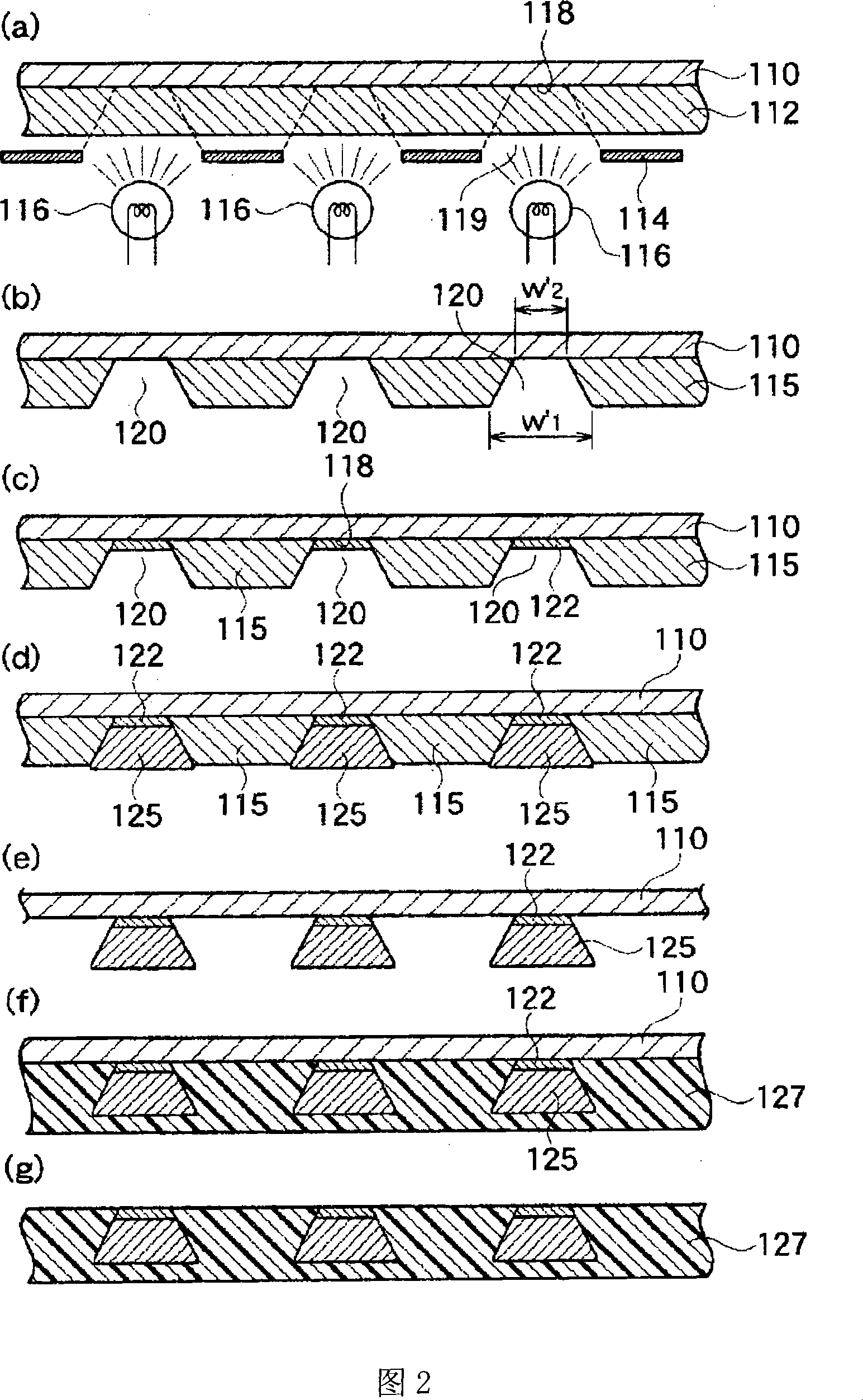
[0200] Using a roll coater, a positive photoresist (manufactured by RomandHaus Co., Ltd., FR200-8cp) was coated with a thickness of 6 μm on an electrolytic copper foil with a width of 48 mm and a thickness of 35 μm (Mitsui Sinzoku) as a support. Mining Co., Ltd. product, VLP copper foil), after drying and curing at 100°C for 1 minute, a pattern with a pitch of 20 μm was drawn on the resist using an exposure developing device.
[0201] Use an exposure device with a wavelength of 365nm, a wavelength of 405nm, and a wavelength of 436nm as the main wavelength (manufactured by Yoshio Electric Co., Ltd., EP-70SAC-02, illuminance: 64mW / cm 2 ), at 630mJ / cm 2 The energy density was exposed, and then developed with 1.5% KOH solution for 65 seconds. The bottom opening is 6.9 μm, and the upper opening is 12.2 μm.
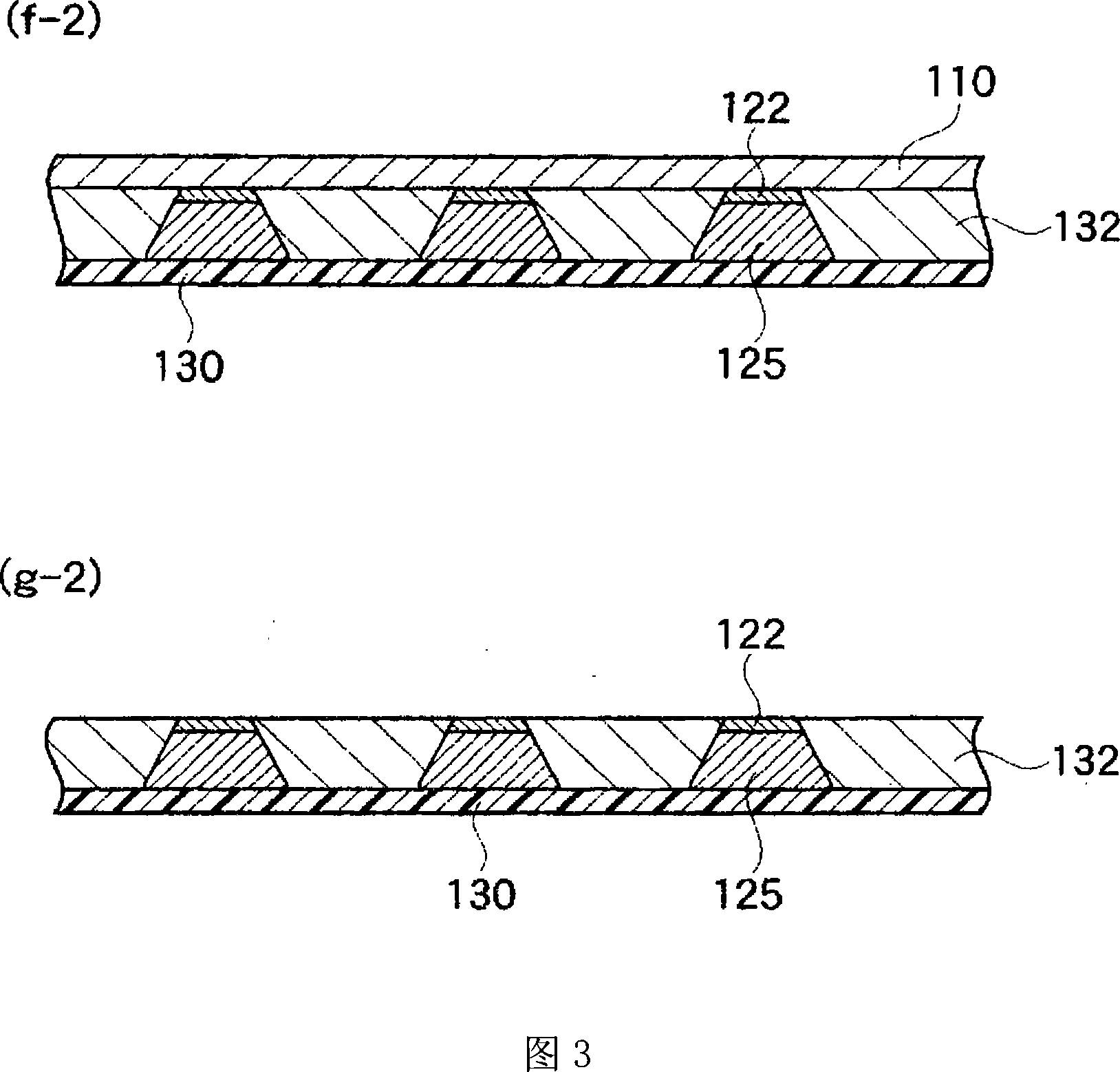
[0202]Then, using a gold plating solution (manufactured by EEJA, Tempelex #8400), at 65°C, DK=0.2A / dm 2 Electroplating was carried out for 1 minute under the condition of , ...
Embodiment 2
[0212] Using a roll coater, a positive photoresist (manufactured by RomandHaus Co., Ltd., trade name FR200-8CP) was coated with a thickness of 6.8 μm on an electrolytic copper foil with a width of 70 mm and a thickness of 35 μm as a support. (manufactured by Mitsui Metal Mining Co., Ltd., trade name: VLP copper foil), after drying and curing at 100° C. for 1 minute, a pattern at a pitch of 20 μm was drawn on this resist using an exposure device.
[0213] Use an exposure device with a wavelength of 365nm, a wavelength of 405nm, and a wavelength of 436nm as the main wavelength (manufactured by Yoshio Electric Co., Ltd., EP-70SAC-02, illuminance: 64mW / cm 2 ), with 630mJ / cm 2 The energy density was exposed, and then developed with 1.5% KOH solution for 65 seconds. The bottom opening is 6.2 μm, and the upper opening is 11.5 μm.
[0214] Then, using a gold plating solution (manufactured by EEJA, Tempelex #8400), at 65°C, DK=0.2A / dm 2 Gold plating was carried out for 1 minute unde...
Embodiment 3
[0224] On a PET film with a width of 48 mm and a thickness of 50 μm with an adhesive, a 3 μm thick electrolytic copper foil (Mitsui Metal Mining Co., Ltd., Microsin copper foil (extremely thin copper foil)) was laminated to prepare a two-layer laminated film. Using an etchant at 40° C. with a nozzle height of 15 cm, the two-layer laminated film was spray-etched for 20 seconds so that the thickness of the copper foil was 1 μm. The composition of the etching solution used here is adjusted within the range of hydrochloric acid 85.4-87.6 g / L, Cu ion concentration 115-135 g / L, and specific gravity 1.250-1.253. The etchant is sprayed with two nozzles, and the pressure adjusted to each nozzle is 2kg / cm 2 , The flow rate of each nozzle is 1.83 liters per minute.
[0225] Using a roll coater, a positive-type photoresist (manufactured by RomandHaus Co., Ltd., FR200-8CP) was applied to a thickness of 6.5 μm on the surface of the half-etched copper foil, and dried and cured at 100° C. fo...
PUM
 Abstract
Description
Claims
Application Information