Simulation image signal processing method for CMOS imaging sensor and circuit thereof

A signal processing circuit, image sensor technology, applied in the direction of image communication, television, electrical components, etc., can solve the problem of not completely eliminating FPN noise, increasing chip area, restricting product miniaturization, etc.

Active Publication Date: 2008-02-27
BYD SEMICON CO LTD
View PDF0 Cites 17 Cited by
  • Summary
  • Abstract
  • Description
  • Claims
  • Application Information

AI Technical Summary

Problems solved by technology

The front-end image signal processing circuit of the existing CMOS image sensor uses multiple circuit modules or multi-level circuits to provide red, green 1 color, green 2 colors, and blue (referred to as R, G1, G2, B) signals to the pixel matrix respectively. For exposure gain control, colo

Method used


Image

  • Simulation image signal processing method for CMOS imaging sensor and circuit thereof
  • Simulation image signal processing method for CMOS imaging sensor and circuit thereof
  • Simulation image signal processing method for CMOS imaging sensor and circuit thereof

Examples


Embodiment Construction

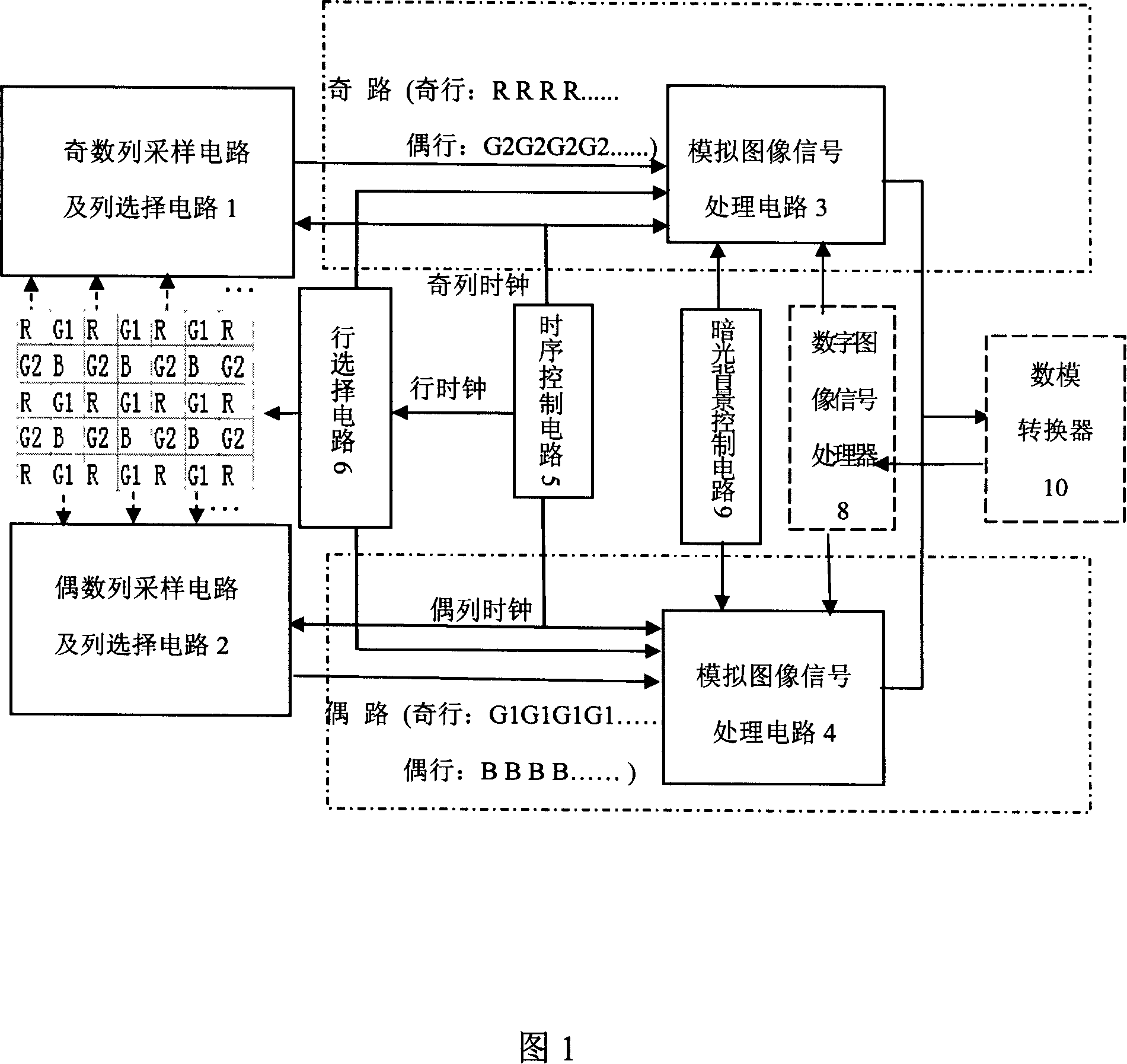
[0047] A kind of analog image signal processing circuit of CMOS image sensor

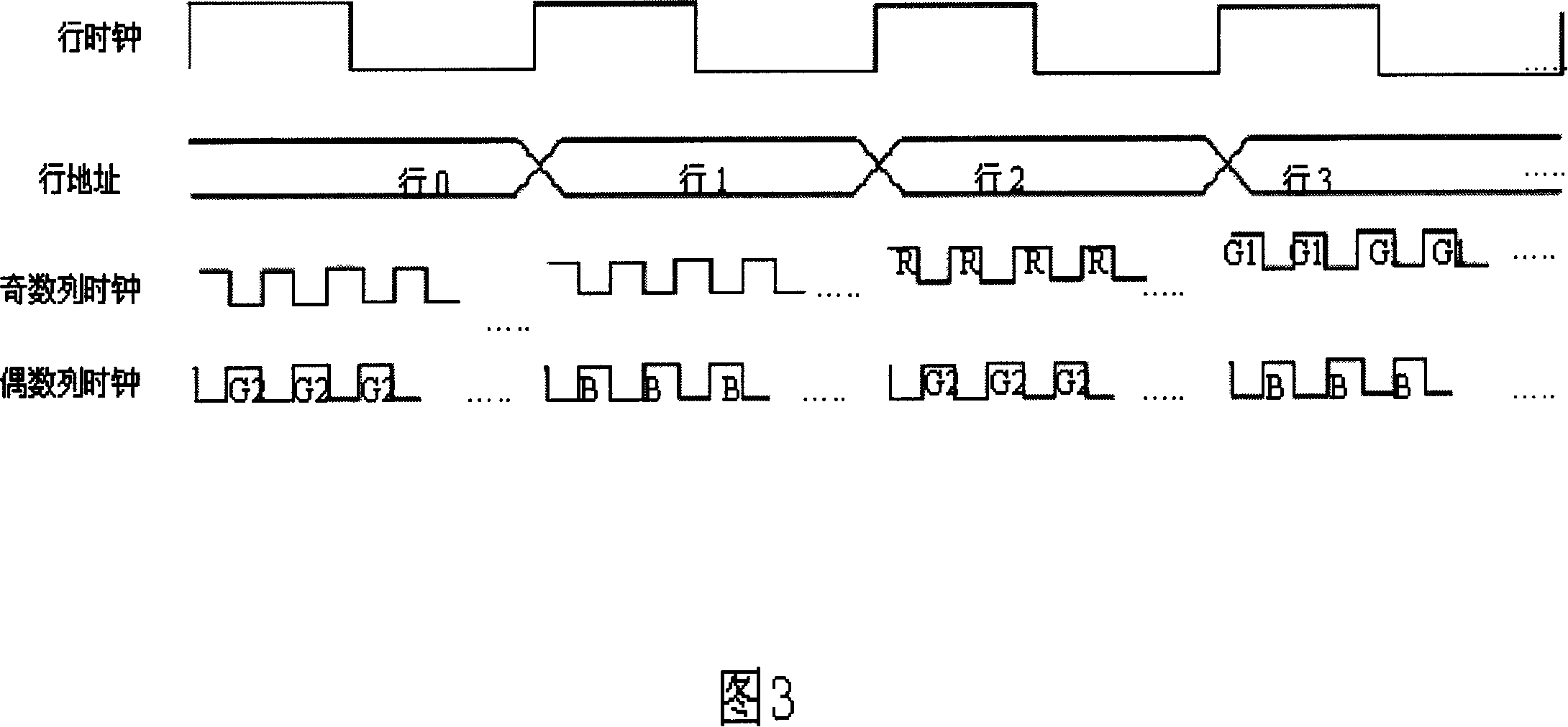
[0048] There are odd and even column pixel sampling and column selection circuits 1 and 2 respectively connected to the odd and even columns of the pixel matrix of the CMOS image sensor, and the odd and even column pixel sampling and column selection circuits 1 and 2 respectively The connected two-way symmetrical odd-numbered and even-numbered pixel analog image signal processing circuits 3 and 4 divide the image signal into two roads for processing respectively according to the odd-numbered and even-numbered columns of the image array.

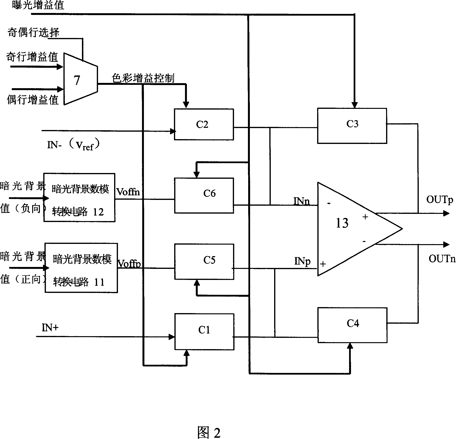
[0049] Odd and even column pixel sampling and column selection circuits 1 and 2 single-end output serial voltage image signals. The pixel analog image signal processing circuits 3 and 4 of odd and even columns are respectively a first-stage switched capacitor differential operational amplifier circuit 13 . The input signal of each analog image signal processing ci...


PUM


Abstract

This invention discloses a method for precessing analog image signals and its circuit of CMOS image sensor, which divides a pixel matrix into two symmetric odd and even arrays and sends related double sample values of each pixel signal to related two symmetric odd and even aray pixel simmulation image signal process circuits composed of a primary switch capacitance difference operation amplifying circuit only orderly at positive and negative half cycles of a line clock to carry out subtraction operation to eliminate dynamic noise and fixed mode noise of the circuit generated by the difference of sample circuits in different ranks and their drive circuit devices and realize control of color gain, exposal gain and dark background not influenced by the exposal background contol.

Description

technical field [0001] The invention relates to general image data processing, in particular to an analog image signal processing method and circuit of a CMOS image sensor which occupies a dominant position in low-end image and video information products. Background technique [0002] A signal processing circuit of an existing Complementary Metal-Oxide-Semiconductor Transistor Image Sensor (CMOS image sensor for short) includes a front-end analog image signal processing circuit and a back-end digital image signal processing circuit. The front-end analog image signal processing circuit includes a correlated double sampling (Correlate Doubled Sampling, referred to as CDS) circuit that can eliminate circuit fixed pattern noise (Fixed Pattern Noise, referred to as FPN), a color gain control circuit, an exposure control circuit and a dark background control circuit; The back-end digital image signal processing circuit includes an analog-to-digital converter and a digital image si...

Claims


Application Information

Patent Timeline
IPC IPC(8): H04N5/335H04N3/15H04N5/243
Inventor 胡文阁
Owner BYD SEMICON CO LTD
Why Eureka
Try Eureka