Supercharge Your Innovation With Domain-Expert AI Agents!

Apparatus for controlling plasma etching process

A technology of plasma etching and control devices, which is applied in the fields of plasma, semiconductor/solid-state device manufacturing, electrical components, etc.

Active Publication Date: 2010-07-28
TAIWAN SEMICON MFG CO LTD
View PDF3 Cites 2 Cited by
  • Summary
  • Abstract
  • Description
  • Claims
  • Application Information

AI Technical Summary

Problems solved by technology

[0006] Therefore, although the existing technology is sufficient to achieve the expected effect under general conditions, it still cannot meet the full range of requirements

Method used


Image

  • Apparatus for controlling plasma etching process
  • Apparatus for controlling plasma etching process
  • Apparatus for controlling plasma etching process

Examples


Embodiment Construction

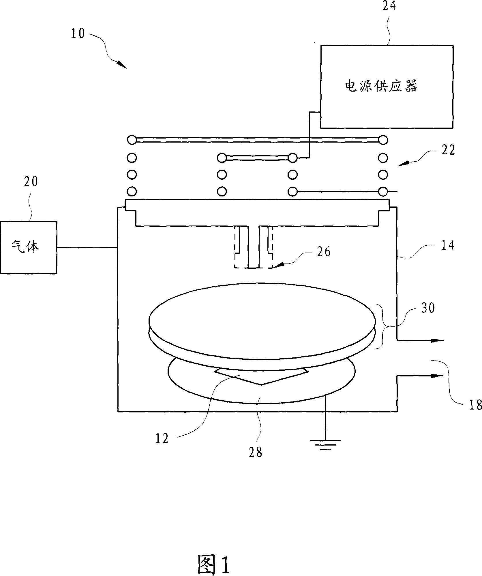
[0068] figure 1 A schematic diagram of a plasma etching system 10 of the present invention. The plasma etching system 10 is used to etch the wafer 12, and can also be used to etch a mask or other objects. The material of the wafer 12 is silicon, or may also contain other elemental semiconductors, such as germanium. Wafer 12 may also comprise compound semiconductors, such as silicon carbide, gallium arsenide, indium arsenide, or indium phosphide. Wafer 12 may also include alloy semiconductors, such as silicon germanium, silicon germanium carbide, gallium arsenide phosphide, or gallium indium phosphide. The wafer 12 may include an epitaxial layer, for example, the wafer 12 has an epitaxial layer covering the bulk semiconductor. Furthermore, the wafer 12 may include a semiconductor-on-insulator (SOI) structure. For example, the wafer 12 may include a structure such as separation by implanted oxygen (SIMOX) ) Oxide buried layer (buried oxide) formed by a process such as The ...


PUM


Abstract

An apparatus for controlling a plasma etching process includes plasma control structure that can vary a size of a plasma flow passage, vary a speed of plasma flowing through the plasma flow passage, vary plasma concentration flowing through the plasma flow passage, or a combination thereof.

Description

technical field [0001] The invention relates to a semiconductor process, in particular to a control device and method used for etching objects with plasma. Background technique [0002] In integrated circuit manufacturing technology, a photoresist layer is generally applied on the surface of a semiconductor wafer before exposing the photoresist through a mask. Then, a post-exposure baking process and a developing process are performed to form a patterned photoresist layer with a plurality of holes. After the above photoresist layer is verified by manufacturing specifications, the exposed part of the wafer is etched by using the above holes. After the wafer is etched, the photoresist layer is removed. [0003] The dry etching process is one of the techniques used to remove the portion of the wafer exposed through the holes in the photoresist layer. One representative example of the dry etching technology is the well-known plasma etching process. Plasma etching is often us...

Claims


Application Information

Patent Timeline
Patent Type & Authority Patents(China)
IPC IPC(8): H01L21/00H01L21/02H01L21/3065H01L21/67C23F4/00H05H1/00H01J37/32
CPCH01J37/32623H01J37/32697
Inventor 张世明吕启纶
Owner TAIWAN SEMICON MFG CO LTD
Features
  • R&D
  • Intellectual Property
  • Life Sciences
  • Materials
  • Tech Scout
  • Unparalleled Data Quality
  • Higher Quality Content
  • 60% Fewer Hallucinations
Learn More