Supercharge Your Innovation With Domain-Expert AI Agents!

Apparatus for controlling plasma etching process

A technology of plasma etching and control devices, which is applied in the fields of plasma, semiconductor/solid-state device manufacturing, electrical components, etc., and can solve problems such as inability to meet all-round requirements

Active Publication Date: 2008-04-30
TAIWAN SEMICON MFG CO LTD
View PDF0 Cites 6 Cited by
  • Summary
  • Abstract
  • Description
  • Claims
  • Application Information

AI Technical Summary

Problems solved by technology

[0006] Therefore, although the existing technology is sufficient to achieve the expected effect under general conditions, it still cannot meet the full range of requirements

Method used


Image

  • Apparatus for controlling plasma etching process
  • Apparatus for controlling plasma etching process
  • Apparatus for controlling plasma etching process

Examples


Embodiment Construction

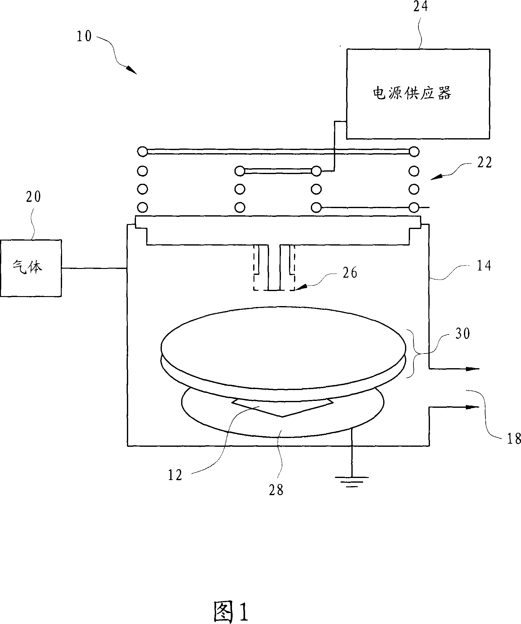
[0069] In order to further explain the technical means and effects of the present invention to achieve the intended purpose of the invention, the specific implementation, structure, features and characteristics of the plasma etching process control device proposed in accordance with the present invention will be described with reference to the accompanying drawings and preferred embodiments. Its efficacy is described in detail later.

[0070] FIG. 1 is a schematic diagram of a plasma etching system 10 of the present invention. The plasma etching system 10 is used to etch the wafer 12, and can also be used to etch masks or other objects. The material of the wafer 12 is silicon, or other element semiconductors, such as germanium. The wafer 12 may also contain compound semiconductors, such as silicon carbide, gallium arsenide, indium arsenide, or indium phosphide. The wafer 12 may also include alloy semiconductors, such as silicon germanium, silicon germanium carbide, gallium arsenid...


PUM


Abstract

An apparatus for controlling a plasma etching process includes plasma control structure that can vary a size of a plasma flow passage, vary a speed of plasma flowing through the plasma flow passage, vary plasma concentration flowing through the plasma flow passage, or a combination thereof.

Description

Technical field [0001] The invention relates to a semiconductor process, in particular to a control device and method used when plasma is used to etch objects. Background technique [0002] In integrated circuit manufacturing technology, generally, a photoresist layer is applied on the surface of the semiconductor wafer before the photoresist is exposed through a photomask. Then, a post-exposure baking process and a development process are performed to form a patterned photoresist layer with a plurality of holes. After the above-mentioned photoresist layer is verified by the manufacturing specifications, the above-mentioned holes are used to etch the exposed part of the wafer. After the wafer is etched, the photoresist layer is removed. [0003] The dry etching process is one of the techniques used to remove the exposed part of the wafer through the hole of the photoresist layer. One of the representative examples of dry etching technology is the well-known plasma etching process...

Claims


Application Information

Patent Timeline
Patent Type & Authority Applications(China)
IPC IPC(8): H01L21/00H01L21/02H01L21/3065H01L21/67C23F4/00H05H1/00H01J37/32
CPCH01J37/32623H01J37/32697
Inventor 张世明吕启纶
Owner TAIWAN SEMICON MFG CO LTD
Features
  • R&D
  • Intellectual Property
  • Life Sciences
  • Materials
  • Tech Scout
  • Unparalleled Data Quality
  • Higher Quality Content
  • 60% Fewer Hallucinations
Learn More