
Fin-fet device with a void between pairs of fins and method of manufacturing the same

A technology of semiconductors and devices, applied in the field of non-volatile memory devices, can solve problems such as interference during read operation, reducing fin distance, etc.

Inactive Publication Date: 2008-05-21
SAMSUNG ELECTRONICS CO LTD
View PDF0 Cites 22 Cited by
  • Summary
  • Abstract
  • Description
  • Claims
  • Application Information

AI Technical Summary

Problems solved by technology

Furthermore, as the integration density of semiconductor devices increases, the distance between fins decreases, causing disturbance during read operations

Method used


Image

  • Fin-fet device with a void between pairs of fins and method of manufacturing the same
  • Fin-fet device with a void between pairs of fins and method of manufacturing the same
  • Fin-fet device with a void between pairs of fins and method of manufacturing the same

Examples


Embodiment Construction

[0013] Exemplary embodiments will now be described more fully with reference to the accompanying drawings. Example embodiments may, however, be embodied in many different forms and should not be construed as limited to the examples set forth herein. The size of elements in the drawings may be exaggerated for illustrative purposes.

[0014] It will be understood that when an element or layer is referred to as being "on," "connected to," "bonded to" or "covering" another element or layer, The element or layer may be directly on, directly connected to, directly bonded to, or directly over said another element or layer, or may be There are intermediate elements or layers. In contrast, when an element is referred to as being "directly on," "directly connected to" or "directly coupled to" another element or layer, there are no intervening elements or layers present. Like reference numerals refer to like elements throughout. As used herein, the term "and / or" includes any and all ...


PUM


Abstract

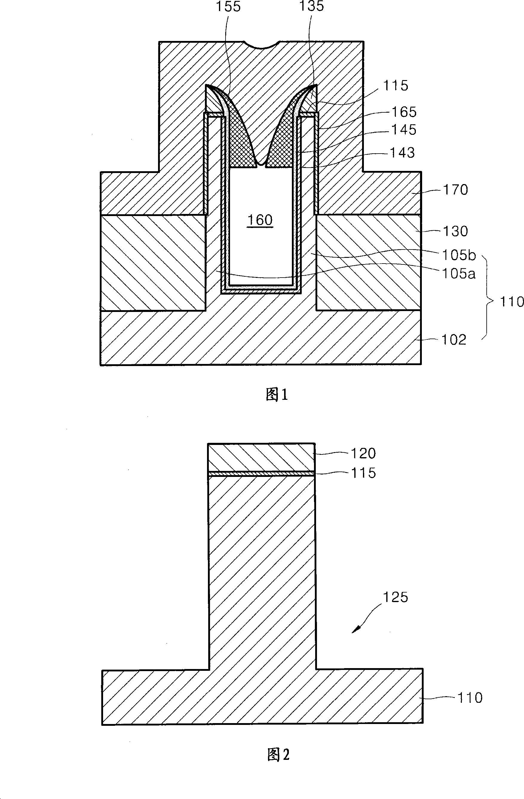
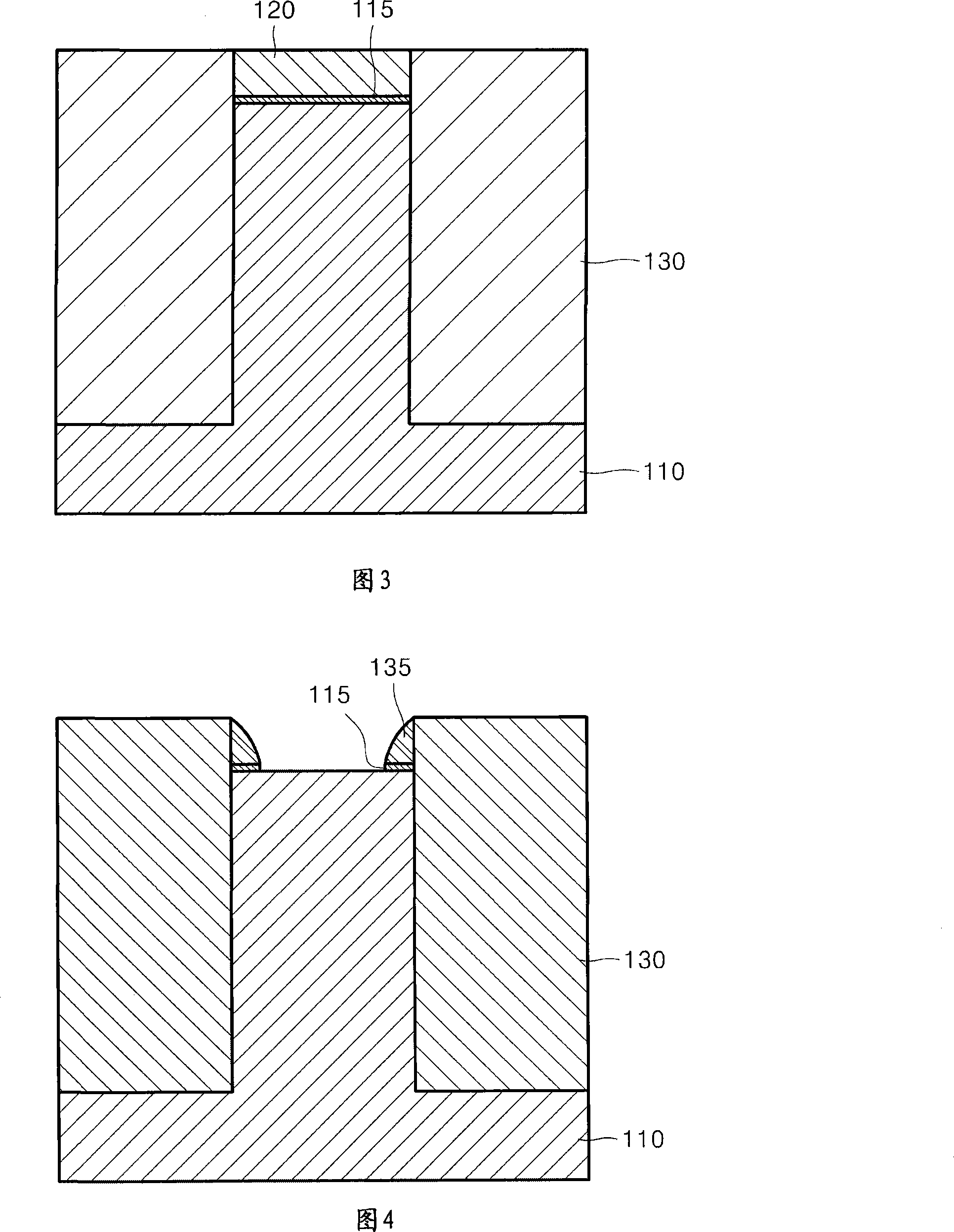
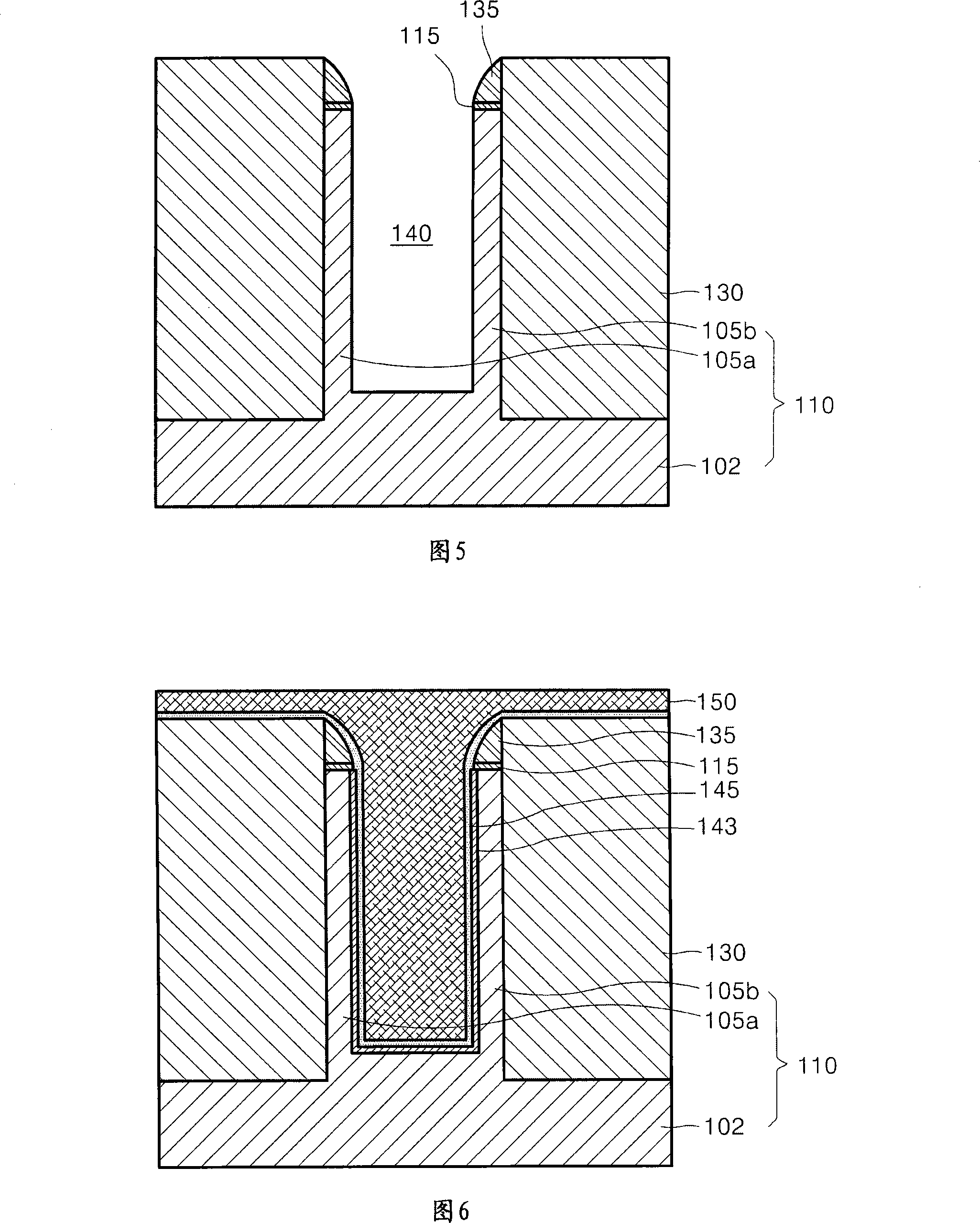
Example embodiments relate to a semiconductor device and a method of manufacturing the same. A semiconductor device according to example embodiments may have reduced disturbances during reading operations and a reduced short channel effect. The semiconductor device may include a semiconductor substrate having a body and a pair of fins protruding from the body. Inner spacer insulating layers may be formed on an upper portion of an inner sidewall of the pair of fins so as to reduce the entrance to the region between the pair of fins. A gate electrode may cover a portion of the external sidewalls of the pair of fins and may extend across the inner spacer insulating layers so as to define a void between the pair of fins. Gate insulating layers may be interposed between the gate electrode and the pair of fins.

Description

technical field [0001] Exemplary embodiments relate to a nonvolatile memory device including a fin-type channel region and a method of manufacturing the same. Background technique [0002] As the size of semiconductor products is further reduced, semiconductor products may require a larger volume of data processing. Accordingly, it would be beneficial to increase the operating speed and integration density of nonvolatile memory devices used in semiconductor products. For example, a semiconductor device having a FinFET structure may have a larger channel surface and thus may have an increased operating speed. Meanwhile, the integration density can be increased by reducing the width of the fins of the FinFET structure. [0003] Fin FETs using silicon-on-insulator (SOI) substrates can improve the short-channel effect. However, SOI substrates can be relatively expensive. In addition, even with SOI substrates, depending on the dielectric properties of the insulator, short-cha...

Claims


Application Information

Patent Timeline
IPC IPC(8): H01L27/115H01L27/088H01L21/8247H01L21/8234
CPCH01L21/28141H01L29/40114H01L29/78603
Inventor 金锡必朴允童李钟振金元柱具俊谟宋承桓
Owner SAMSUNG ELECTRONICS CO LTD
Learn More