

Semiconductor device and method for manufacturing the same
a semiconductor and semiconductor technology, applied in the direction of semiconductor devices, basic electric elements, electrical appliances, etc., can solve the problems of increasing the probability of occurrence of defective products, the atomic radius of ion species used in the plasma treatment of oxide semiconductors, and the inability to manufacture over a larger glass substrate, so as to improve the on-state current and increase the transistor on-state current
- Summary
- Abstract
- Description
- Claims
- Application Information
AI Technical Summary
Benefits of technology
Problems solved by technology
Method used
Image

Examples
embodiment 1
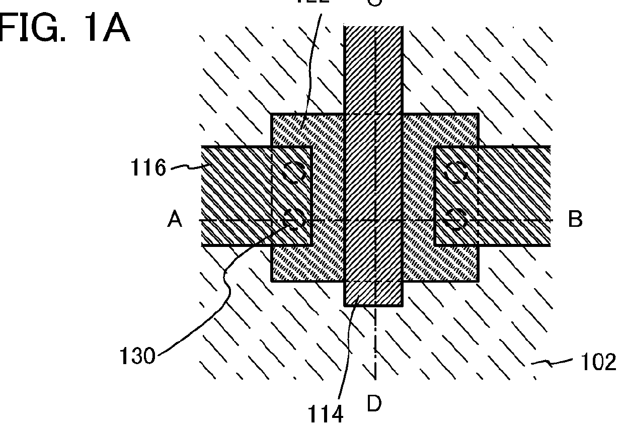
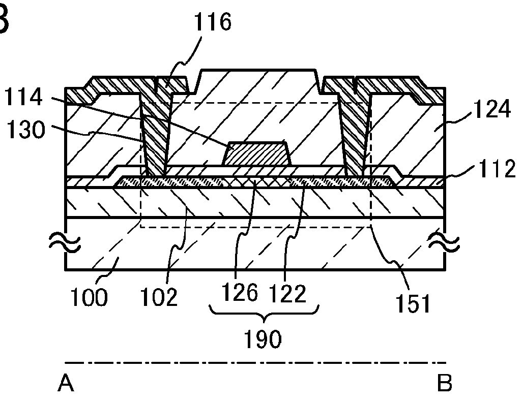
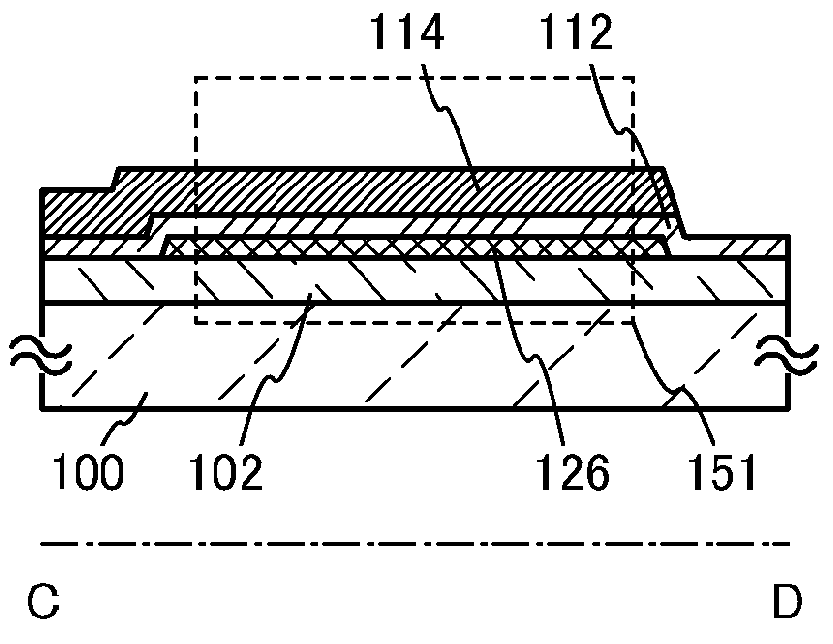
[0053]In this embodiment, an example of a top-gate transistor in which a channel region is formed using a first oxide semiconductor region to which ions are not added, and a source region and a drain region are formed using second oxide semiconductor regions to which ions are added and which are in the same layer as the channel region will be described with reference to FIGS. 1A to 1C and FIGS. 2A to 2D.
[0054]FIGS. 1A to 1C are a top view and cross-sectional views of a top-gate transistor. Here, FIG. 1A is a top view, FIG. 1B is a cross-sectional view taken along A-B in FIG. 1A, and FIG. 1C is a cross-sectional view taken along C-D in FIG. 1A. Note that in FIG. 1A, some components of a transistor 151 (e.g., a gate insulating film 112 and an interlayer insulating film 124) are omitted for simplicity.
[0055]The transistor 151 illustrated in FIGS. 1A to 1C includes an oxide semiconductor film 190 over an insulating surface which includes a first oxide semiconductor region 126 and a pair...
embodiment 2
[0123]In this embodiment, an example of a transistor which is different from the transistor described in Embodiment 1 will be described with reference to FIG. 3 and FIGS. 4A to 4D.
[0124]A transistor 152 illustrated in FIG. 3 includes a base insulating film 102 over a substrate 100, source and drain electrodes 216 over the base insulating film 102, an oxide semiconductor film 290 over the base insulating film 102 which includes a first oxide semiconductor region 226 and a pair of second oxide semiconductor regions 222 connected to the source and drain electrodes 216, a gate insulating film 212 over the oxide semiconductor film 290, a gate electrode 214 over the gate insulating film 212, and an interlayer insulating film 224 over the gate insulating film 212 and the gate electrode 214.
[0125]The channel length of the transistor is determined by the distance between the pair of second oxide semiconductor regions 222. The channel length is preferably equal to the width of the gate electr...
embodiment 3
[0135]In this embodiment, an example of a transistor which is different from the transistors described in Embodiments 1 and 2 will be described with reference to FIG. 5 and FIGS. 6A to 6D.
[0136]A transistor 153 illustrated in FIG. 5 includes a substrate 100 having an insulating surface, a gate electrode 314 over the substrate 100, a gate insulating film 312 over the gate electrode 314, an oxide semiconductor film 390 which is provided over the gate electrode 314 with the gate insulating film 312 interposed therebetween and includes a first oxide semiconductor region 326 and a pair of second oxide semiconductor regions 322, an insulating film 319 which is provided over and to overlap with the first oxide semiconductor region 326, source and drain electrodes 316 connected to the pair of second oxide semiconductor regions 322, and an interlayer insulating film 324 over the insulating film 319 and the source and drain electrodes 316. Note that a base insulating film 102 may be provided ...
PUM
 Abstract
Description
Claims
Application Information