Surround gate access transistors with grown ultra-thin bodies

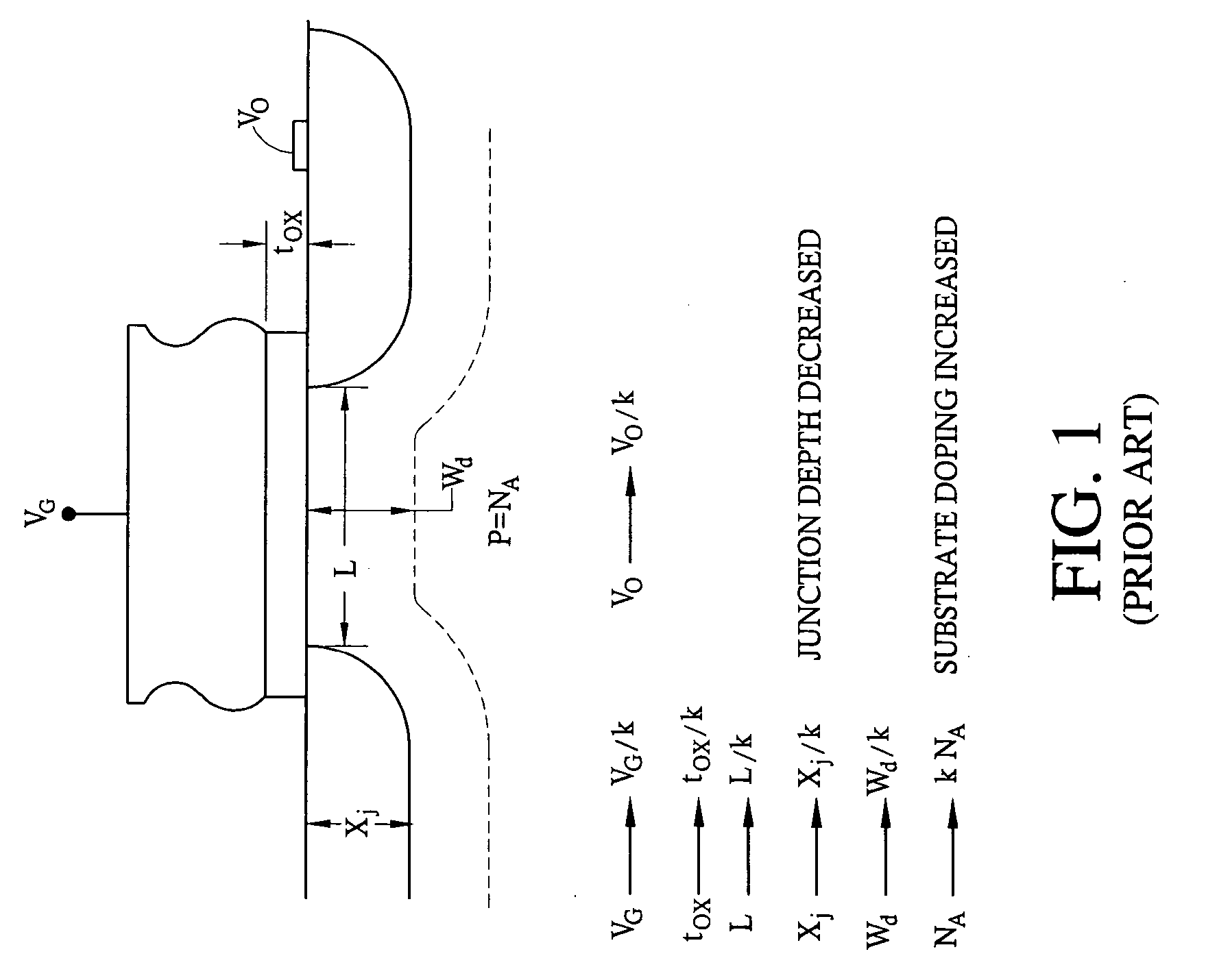
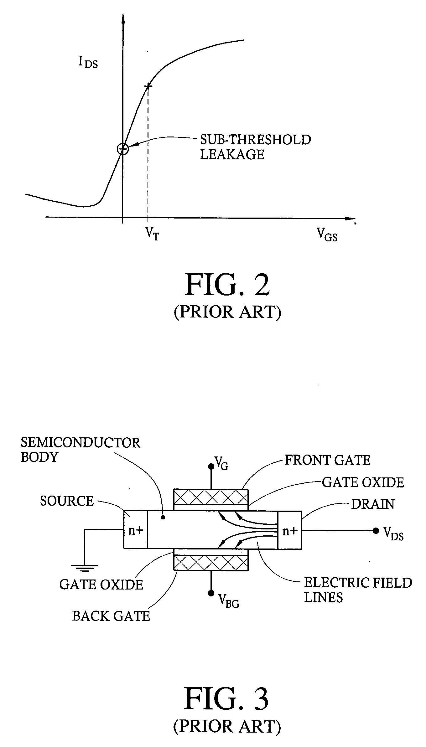
a technology of access transistors and surround gate access transistors, which is applied in the field of access transistors with grown ultra-thin bodies, can solve the problems of difficult formation of shallow junctions, significant problems in conventional transistor structures, and particularly problematic sub-threshold conduction

Active Publication Date: 2007-01-25
MICRON TECH INC
View PDF98 Cites 61 Cited by
  • Summary
  • Abstract
  • Description
  • Claims
  • Application Information

AI Technical Summary

Benefits of technology

[0009] The aforementioned needs are satisfied by the invention which in one embodiment comprises a transistor comprising a vertical annular semiconductive transistor body, a surround gate structure formed around the annular transistor body, a source region formed adjacent a lower portion of the body, and a drain region formed adjacent an upper portion of the body such that the transistor defines a field effect transistor.

Problems solved by technology

Ongoing scaling of metal oxide semiconductor field effect transistor (MOSFET) technology to the deep sub-micron region where channel lengths are less than 0.1 micron (100 nanometers or 1,000 Å) causes significant problems in conventional transistor structures.
Such shallow junctions are difficult to form by conventional implantation and diffusion techniques.
Sub-threshold conduction is particularly problematic in dynamic random access memory (DRAM), as it significantly reduces the charge storage retention time of the capacitor cells.
Extremely high doping level generally results in increased leakage and reduced carrier mobility.
This leakage current is a significant concern and problem in low voltage and low power battery operated complimentary metal oxide semiconductor (CMOS) circuits and systems, particularly in DRAMs.
FIG. 2 shows that if low voltages are used for this low power operation, there is a problem with threshold voltages and standby leakage current being of large enough value to degrade overall circuit performance.
However the transistor, such as an access transistor, will always have a large sub-threshold leakage current.

Method used


Image

  • Surround gate access transistors with grown ultra-thin bodies
  • Surround gate access transistors with grown ultra-thin bodies
  • Surround gate access transistors with grown ultra-thin bodies

Examples


Embodiment Construction

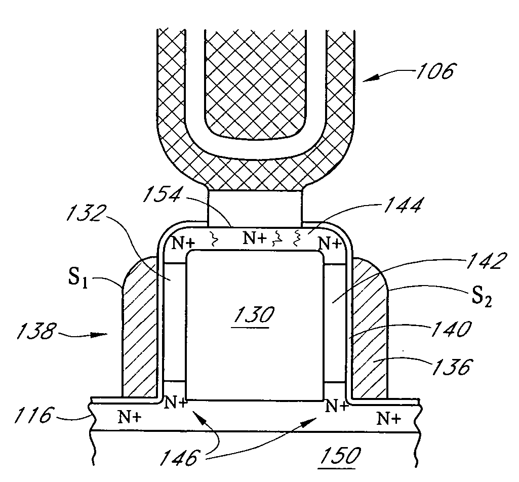
[0025] Description of various embodiments of the invention will now be described with respect to the drawings wherein like reference designators refer to like structures, elements, and / or processes throughout. It should be understood that the illustrations are schematic in nature and should not be interpreted as being to scale. FIG. 5 is a schematic circuit diagram of one embodiment of a memory array 100. The memory array 100 is configured for storage and retrieval of digital data in a plurality of memory cells 102 comprising the array 100. In this embodiment, each memory cell 102 comprises an access transistor 104 connected to a charge storage device 106. In one embodiment, the charge storage device 106 comprises a stacked storage capacitor which will be described in greater detail below. The charged storage devices 106 store the digital data wherein presence of a predetermined quantity of charge on a charge storage device 106 corresponds to a first data state and wherein absence o...


PUM


Abstract

A vertical transistor having an annular transistor body surrounding a vertical pillar, which can be made from oxide. The transistor body can be grown by a solid phase epitaxial growth process to avoid difficulties with forming sub-lithographic structures via etching processes. The body has ultra-thin dimensions and provides controlled short channel effects with reduced need for high doping levels. Buried data/bit lines are formed in an upper surface of a substrate from which the transistors extend. The transistor can be formed asymmetrically or offset with respect to the data/bit lines. The offset provides laterally asymmetric source regions of the transistors. Continuous conductive paths are provided in the data/bit lines which extend adjacent the source regions to provide better conductive characteristics of the data/bit lines, particularly for aggressively scaled processes.

Description

BACKGROUND OF THE INVENTION [0001] 1. Field of the Invention [0002] The invention relates to the field of semiconductor memory arrays and, more particularly, to arrays with access transistors having grown ultra-thin bodies. [0003] 2. Description of the Related Art [0004] Ongoing scaling of metal oxide semiconductor field effect transistor (MOSFET) technology to the deep sub-micron region where channel lengths are less than 0.1 micron (100 nanometers or 1,000 Å) causes significant problems in conventional transistor structures. Generally, junction depth should be much less than the channel length, and thus for a channel length of, for example 1,000 Å, this implies junction depths on the order of a few hundred Angstroms. Such shallow junctions are difficult to form by conventional implantation and diffusion techniques. [0005]FIG. 1 illustrates general trends and relationships for a variety of device parameters with scaling by a factor k. As another example, with an aggressive scaling ...

Claims


Application Information

Patent Timeline
Patent Type & Authority Applications(United States)
IPC IPC(8): H01L29/76
CPCH01L27/10876H01L29/7827H01L29/66666H10B12/053
Inventor FORBES, LEONARD
Owner MICRON TECH INC
Why Eureka
Try Eureka