Semiconductor device having SOI structure and manufacturing method thereof

a semiconductor device and soi technology, applied in the field of structure and manufacturing method of insulatedgate semiconductor devices having soi (silicononinsulator) structure, can solve the problems of difficult control, latch-up phenomenon, and problems where scaling rule does not apply in simple form

Inactive Publication Date: 2008-03-04
SEMICON ENERGY LAB CO LTD
View PDF78 Cites 66 Cited by
  • Summary
  • Abstract
  • Description
  • Claims
  • Application Information

AI Technical Summary

Benefits of technology

[0033]The present invention has been made to solve the above problems in the art, and an object of the invention is therefore to provide a technique for effectively suppressing the short channel effects due to miniaturization of semiconductor elements. The invention is intended to enable formation of very small elements in the deep submicron range which have been difficult to form conventionally due to the short channel effects.
[0040]The main point of the invention is to effectively suppress a depletion layer developing from the drain region toward the channel forming region by the impurity regions that are formed artificially and locally in the channel forming region, to thereby prevent various problems of the short channel effects such as the punch-through phenomenon, deterioration of the subthreshold characteristic, and decrease in breakdown voltage.
[0042]That is, the impurity regions are formed locally in the channel forming region and utilized as energy barriers. By utilizing the impurity regions as energy barriers, the drain region side depletion layer is prevented, in terms of energy, from expanding toward the channel forming region side, whereby an electric field formed in the channel forming region is allowed to be controlled only by the gate voltage.
[0044]The impurity regions formed by adding the above impurity element can shift the energy band of the channel forming region, and thereby change the threshold voltage to the positive or negative side. Therefore, the concentration of the added impurity element should be at least a level that enables threshold voltage control (typically 1×10¹⁷ to 1×10²⁰ atoms / cm3, and preferably 1×10¹⁸ to 1×10¹⁹ atoms / cm3).

Problems solved by technology

Where a CMOS IC is miniaturized, a problem of a latch-up phenomenon may occur between an n-type FET and a p-type FET.
However, in microprocessing in a submicron range, problems may occur where the scaling rule does not apply in simple form.
As a result, the on-current varies depending on a complex electric field profile and is hard to control only by the gate voltage Vg.
Although the reduction in threshold voltage is desirable for the purpose of reducing the power consumption, in general a resulting reduction in the drive voltage of an integrated circuit causes demerits such as a difficulty in improving the frequency characteristic.
Since a large current comes to flow as the drain voltage is increased, the source-drain breakdown voltage is considerably reduced which is a problem.
However, this technique does not provide a complete solution.
However, in such a high-speed semiconductor device, at present, the problems such as the punch-through phenomenon as one of the short channel effects and the associated deterioration in breakdown voltage (described above) remain unsolved.
However, this method has a problem of a reduction in carrier mobility because the added impurity scatters carriers.
However, in a single crystal silicon substrate manufactured by the CZ method, the amount of warp increases due to a heat history and other factors as the oxygen content is reduced.

Method used


Image

  • Semiconductor device having SOI structure and manufacturing method thereof
  • Semiconductor device having SOI structure and manufacturing method thereof
  • Semiconductor device having SOI structure and manufacturing method thereof

Examples


embodiment 1

[0107]In this embodiment, with reference to FIGS. 7A through 12B, a description will be made of a case where insulated-gate field-effect transistors, more specifically, a CMOS circuit as a complementary combination of n-channel and p-channel FETs, are formed on a SIMOX substrate by using the invention.

[0108]First, a single crystal silicon substrate 701 having weak n-type or p-type conductivity is prepared. A buried oxide film 702 is formed by implanting oxygen ions at a dose of 1×10¹⁸ atoms / cm2 and then performing a heat treatment in a temperature range of 800°-1,300° C. Thus, a buried oxide film 702 of 0.05-0.5 μm in thickness and a single crystal silicon layer 703 of 100-2,000 Å in thickness (preferably 200-600 Å) are obtained.

[0109]As one of the most remarkable features of the SOI technology, the single crystal silicon layer 703 has almost no, i.e., only one to several, impurity elements (already contained in the mother substrate 701), and is therefore extremely pure and intrinsi...

embodiment 2

[0172]In the invention, impurity regions may be formed in a channel forming region by utilizing segregation of an impurity. In this embodiment, with reference to FIGS. 13A-13B and 14A-14C, a description will be made of an example of such a method, that is, a method which utilizes segregation of boron (B) or phosphorus (P) in the vicinity of a thermal oxidation film.

[0173]This embodiment is a technique which utilizes a phenomenon that an impurity element (boron or phosphorus) that is contained around the impurity regions (i.e., in the potential slit regions) segregates in the impurity regions. Now, referring to FIGS. 13A and 13B, a description will be made of a boron or phosphorus concentration profile in the vicinity of a thermal oxidation film / silicon interface after execution of a thermal oxidation process.

[0174]As shown in FIGS. 13A and 13B, added ions (B or P) existing in Si are redistributed when an oxide film is formed. This phenomenon is caused by differences in the solubilit...

embodiment 3

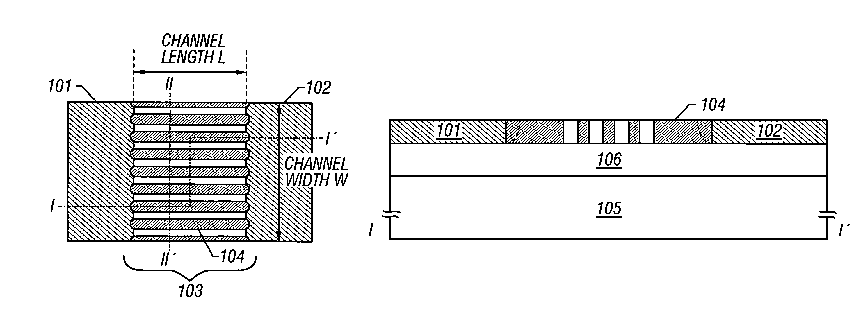
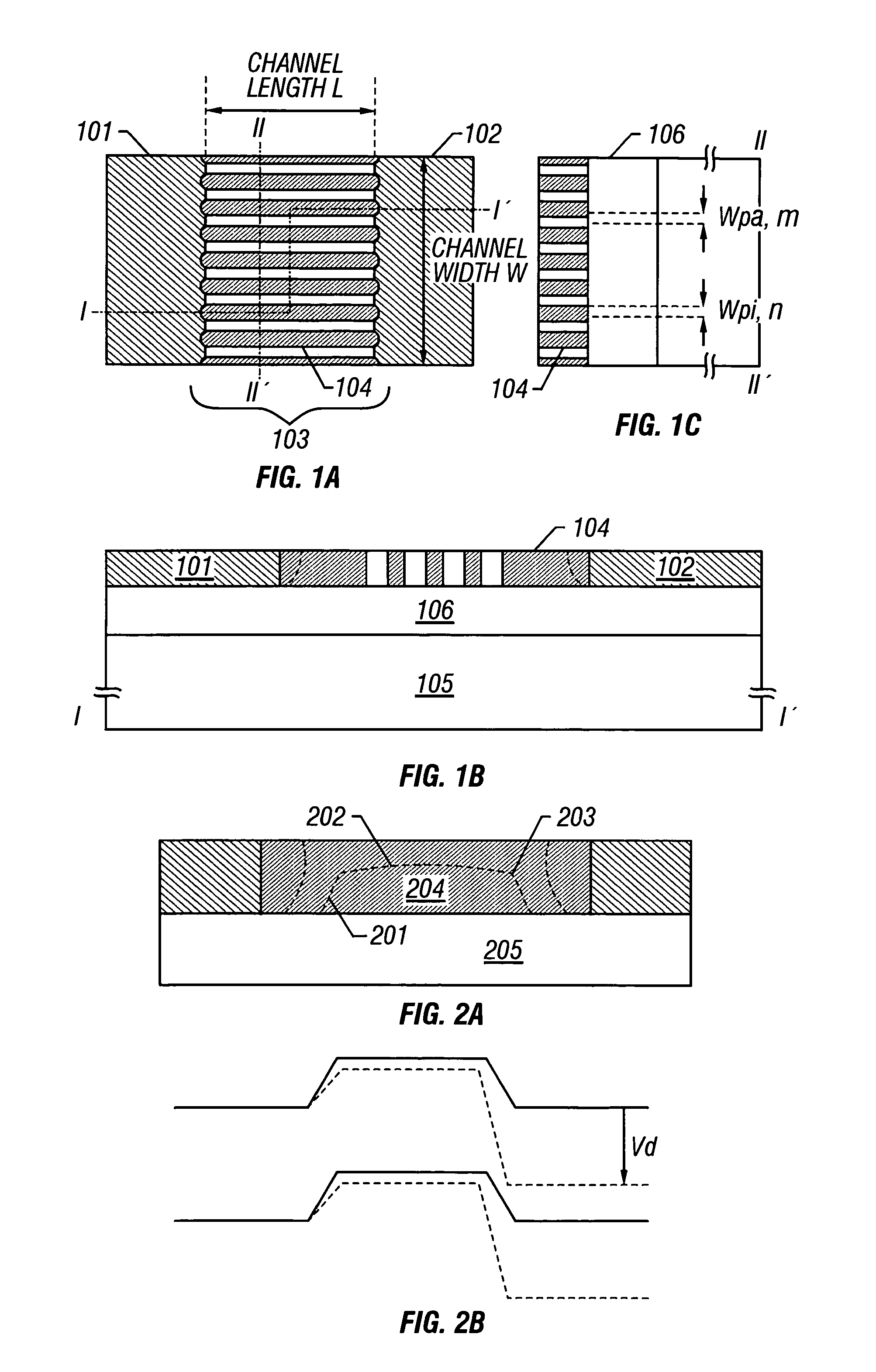
[0191]This embodiment is directed to a case of forming dot-pattered impurity regions in a channel forming region. This embodiment will be described with reference to FIGS. 15A-15C in which the same reference numerals as in FIGS. 1A-1C are used for convenience of description.

[0192]A semiconductor device of FIGS. 15A-15C are configured such that the linearly patterned impurity regions in FIGS. 1A-1C are replaced by dot-patterned ones. That is, impurity regions 1501 are arranged as shown in FIG. 15A.

[0193]FIGS. 15B and 15C are sectional views taken along lines A-A′ and B-B′ in FIG. 15A, respectively.

[0194]Although this embodiment employs circular impurity regions as the dot-patterned impurity regions, the dot-patterned impurity may have an elliptical shape, a square shape, a rectangular shape, or the like.

[0195]The dot-patterned impurity regions do not provide the role of the lane regions of the first embodiment. However, since the effective channel area (carrier movable area) is large...


PUM


Abstract

A fine semiconductor device having a short channel length while suppressing a short channel effect. Linearly patterned or dot-patterned impurity regions 104 are formed in a channel forming region 103 so as to be generally parallel with the channel direction. The impurity regions 104 are effective in suppressing the short channel effects. More specifically, the impurity regions 104 suppress expansion of a drain-side depletion layer, so that the punch-through phenomenon can be prevented. Further, the impurity regions cause a narrow channel effect, so that reduction in threshold voltage can be lessened.

Description

[0001]This is a divisional of U.S. application Ser. No. 08 / 931,697, filed Sep. 16, 1997 (now U.S. Pat. No. 6,127,702).BACKGROUND OF THE INVENTION[0002]1. Field of the Invention[0003]The present invention relates to a structure and a manufacturing method of an insulated-gate semiconductor device having an SOI (silicon-on-insulator) structure, particularly an insulated-gate field-effect transistor (hereinafter referred to simply as IG-FET). An example of the insulated-gate semiconductor device having a SOI structure is a semiconductor device formed on an SOS (silicon-on-sapphire) substrate or a SIMOX (separated-by-implanted oxygen) substrate.[0004]In particular, the invention relates to a technique that is effective in forming a very small element having a channel length of less than 0.35 μm (particularly less than 0.1 μm). Thus, the invention can be applied to various semiconductor integrated circuits such as ICs, VLSIs, and ULSIs that are formed by integrating IG-FETs.[0005]The term...

Claims


Application Information

Patent Timeline
Patent Type & Authority Patents(United States)
IPC IPC(8): H01L29/76H01L29/94H01L27/08B82B1/00H01L21/335H01L21/336H01L21/84H01L27/12H01L29/10H01L29/786
CPCB82Y10/00H01L21/84H01L27/1203H01L29/1041H01L29/66439H01L29/66772H01L29/78654H01L29/78696H01L29/78
Inventor YAMAZAKI, SHUNPEIOHTANI, HISASHIKOYAMA, JUNFUKUNAGA, TAKESHI
Owner SEMICON ENERGY LAB CO LTD
Why Eureka
Try Eureka