Chip test method, system and apparatus

A test equipment and chip testing technology, applied in the field of testing, can solve the problems of not being able to modify the test logic, affecting the test speed, increasing the chip area, etc., to achieve the effect of improving the test speed, reducing the area and reducing the cost

Inactive Publication Date: 2008-06-04
VIMICRO CORP
View PDF0 Cites 5 Cited by
  • Summary
  • Abstract
  • Description
  • Claims
  • Application Information

AI Technical Summary

Problems solved by technology

However, this method needs to add a logic module or test module with functional testing in the chip, which will increase the area of ​​the chip, and when the test module performs the test function, it first needs to be fixed.
In this way, no matter in the development process of the chip or after the chip is manufactured, the test logic cannot be modified according to the new debugging scheme, thereby affecting the test speed

Method used


Image

  • Chip test method, system and apparatus
  • Chip test method, system and apparatus
  • Chip test method, system and apparatus

Examples


Embodiment Construction

[0042] In order to make the object, technical solution and advantages of the present invention clearer, the present invention will be further described in detail below with reference to the accompanying drawings and examples.

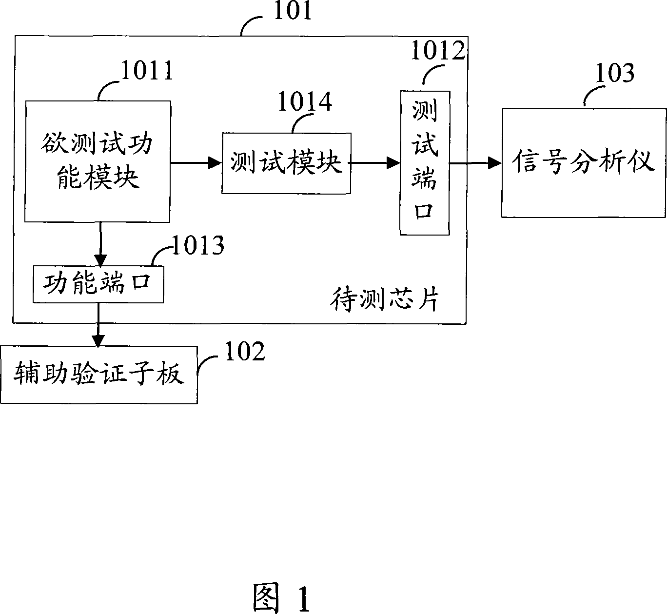
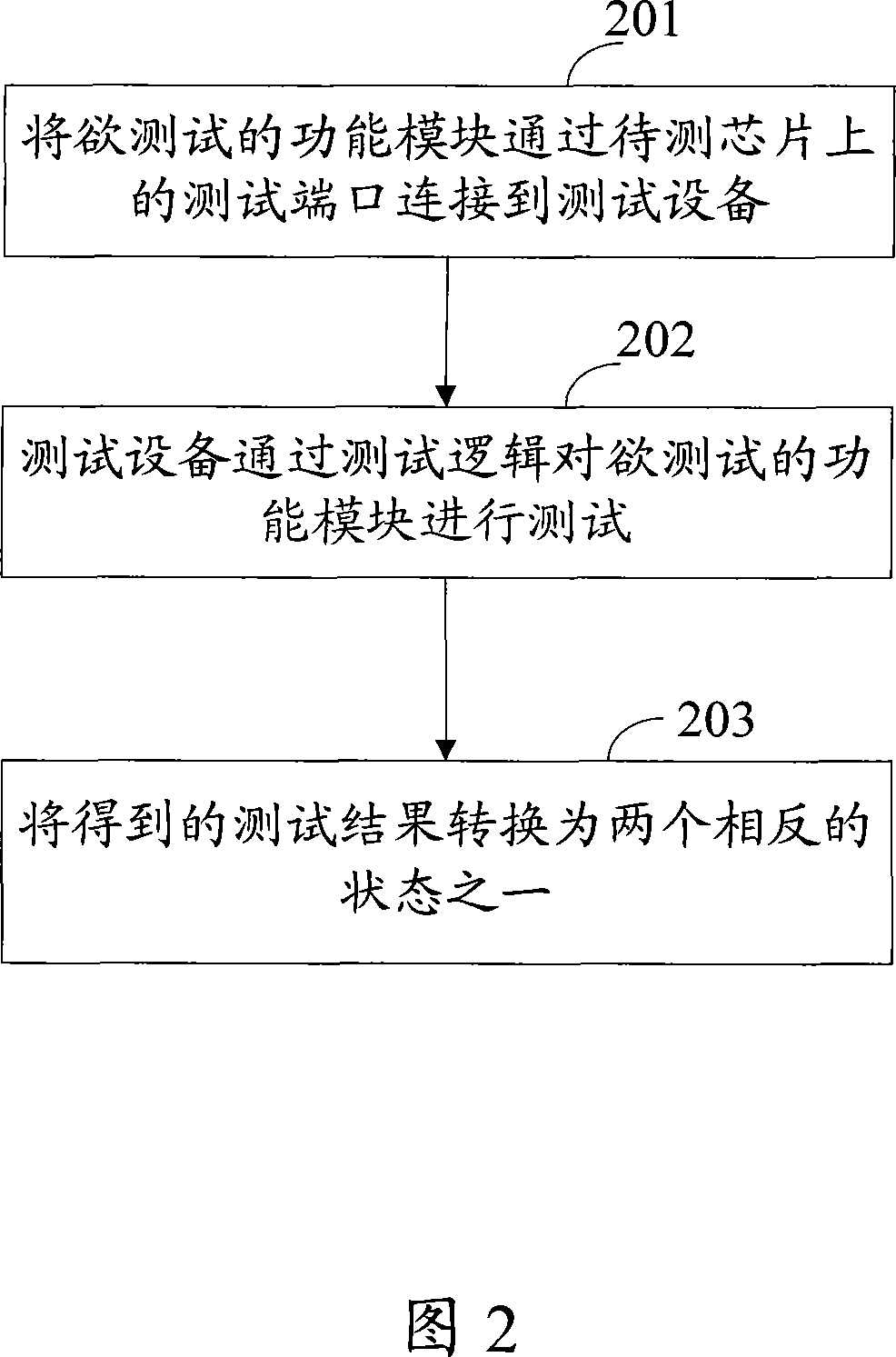
[0043] Different from the prior art, the embodiment of the present invention is to first estimate the errors that may occur in the functional modules to be tested on the chip to be tested; set the test logic for testing the errors, and set the test logic in the in test equipment external to the chip. In this way, the method for testing the chip to be tested in the embodiment of the present invention mainly includes: the test device tests the functional module through the test logic; converts the obtained test result into one of two opposite states, so The two opposite states respectively indicate whether there is an error in the functional module, so that the test logic can be modified according to the new debugging scheme, and the test speed can be imp...


PUM


Abstract

The invention discloses a method for testing chips which comprises the following steps of: preestimating the possible errors in a functional module to be tested of a chip to be tested; setting the test logic for testing the errors and arranging the test logic in a test device arranged outside the chip to be tested. The method also comprises the following steps that: the test device is used to test the functional module by means of the test logic and converts the test result into one of the two states which respectively indicate that errors exist in the functional module and that errors do not exist in the functional module. The invention also discloses a chip testing system and the test device. With the invention, the test logic can be changed according to new test proposal, thereby increasing the test speed.

Description

technical field [0001] The invention relates to testing technology, in particular to a chip testing method, system and testing equipment. Background technique [0002] At present, chip verification testing and debugging occupy more than 70% of the time in the entire chip development process. Usually, there are two main methods for chip testing. The first is software testing, which generates various test incentives for the chip to be tested through computer programming. In this way, the results generated by various test stimuli can be compared with the results expected to be generated by the chip to be tested, thereby verifying the function of the chip to be tested. The second is hardware testing, which is to approximate the actual working environment of the chip to be tested by building a hardware testing platform. In this way, the function of the chip can be verified more realistically. The second method for verifying and testing the chip under test in the prior art wil...

Claims


Application Information

Patent Timeline
Patent Type & Authority Applications(China)
IPC IPC(8): G01R31/28G01R31/3185
Inventor 刘子熹
Owner VIMICRO CORP
Why Eureka
Try Eureka