

Pixel structure and its repairing method
A technology of pixel structure and pixel electrode, applied in the field of pixel structure and its repair
- Summary
- Abstract
- Description
- Claims
- Application Information
AI Technical Summary
Problems solved by technology
Method used
Image

Examples
Embodiment Construction
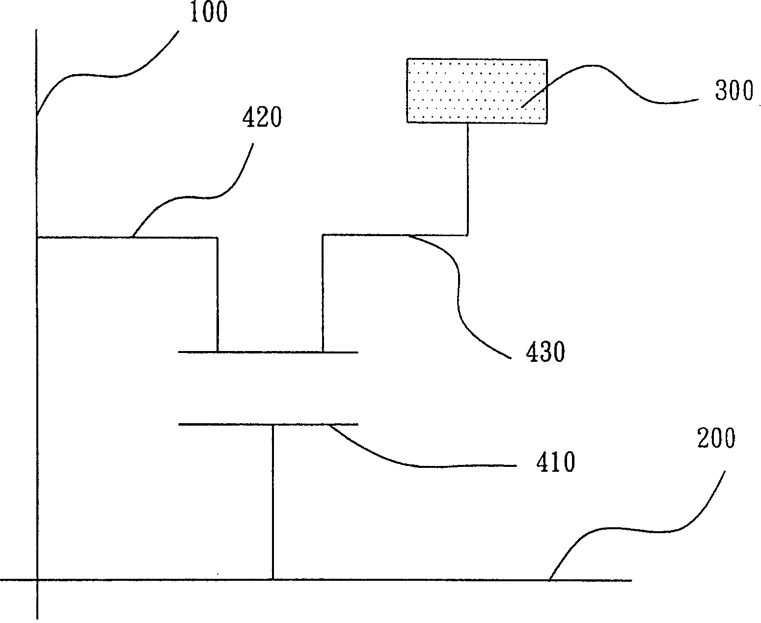
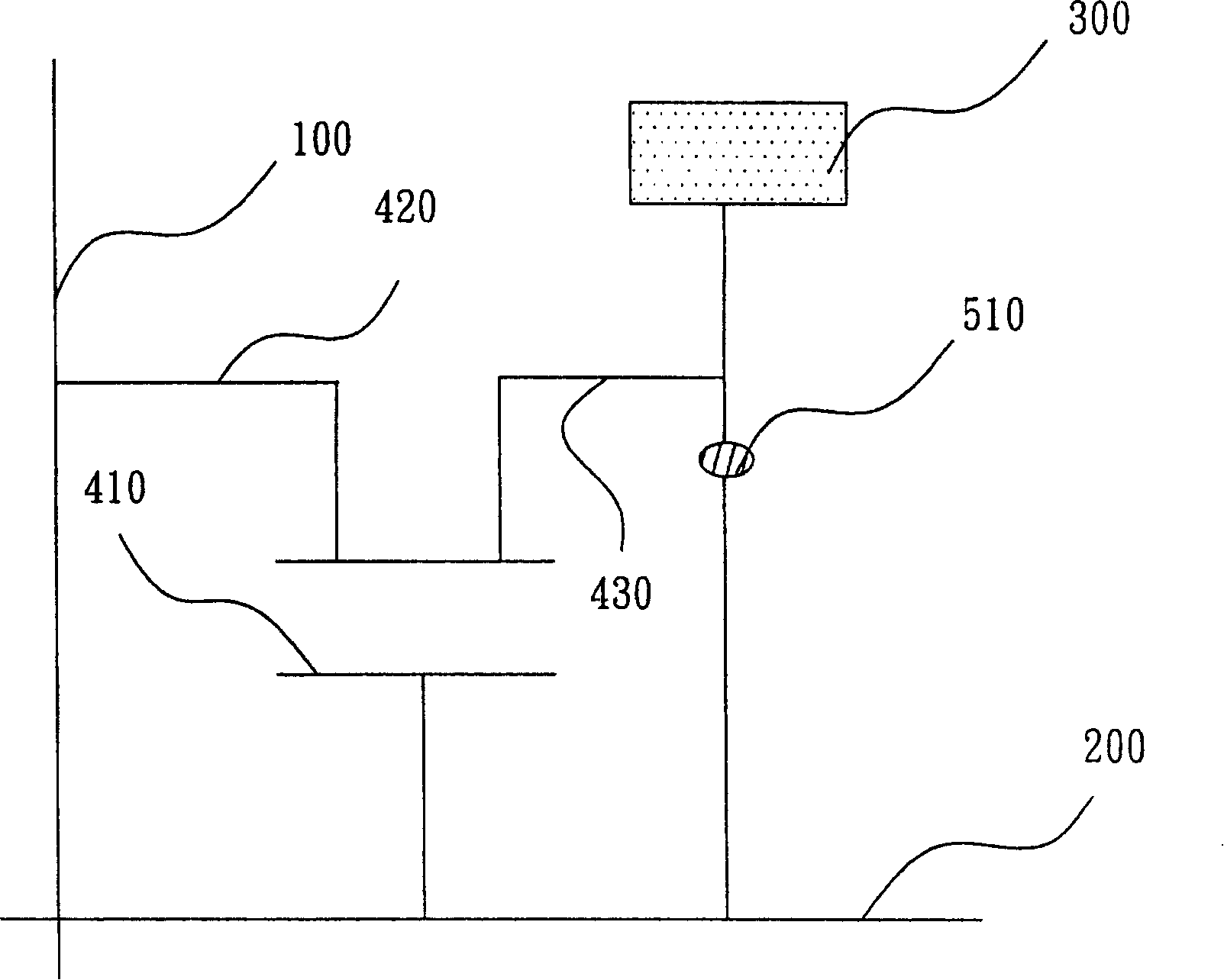
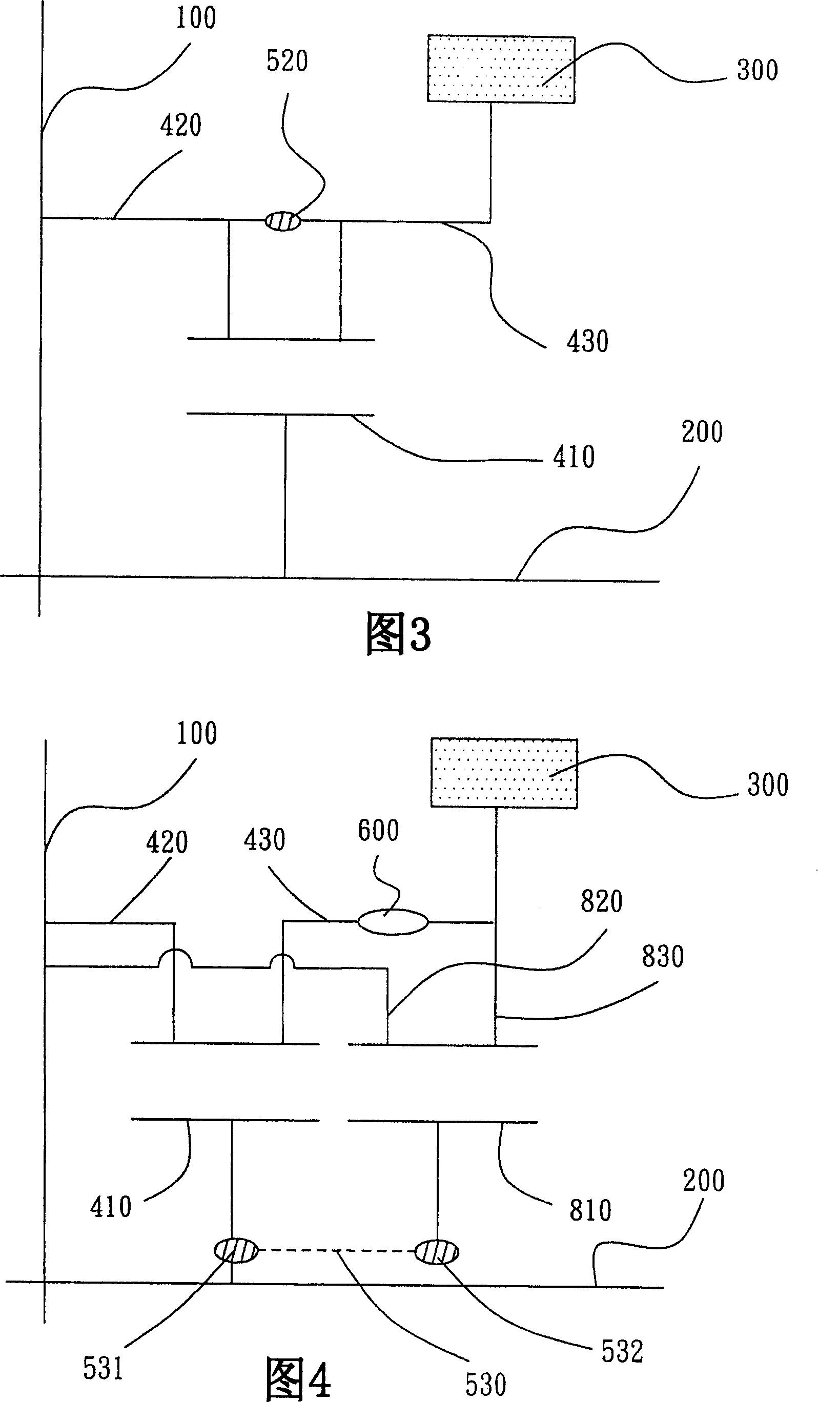
[0037] The pixel structure of the thin film transistor liquid crystal display is arranged on a substrate, and a plurality of data lines and scanning lines are arranged on the substrate to cross to define a plurality of pixel areas, and each pixel area includes a first thin film transistor, a second thin film transistor, A pixel electrode and a repair pattern, wherein the first and second thin film transistors both include a gate, source and drain, the first thin film transistor and the second thin film transistor are driven by the data line and the scanning line, wherein the first thin film transistor The drain of the transistor is electrically connected to the pixel electrode, and the gate or drain of the second thin film transistor remains as an independent metal electrode.
[0038] The method of repairing, when a defective pixel occurs, cut off the pixel electrode and the drain of the first thin film transistor, connect the gate or drain of the first and second thin film tra...
PUM
 Abstract
Description
Claims
Application Information