Mask plate, mask plate layout design method and defect repairing method

A technology of layout design and mask, which is applied in the field of mask, can solve problems such as inability to repair and position, reduce the risk of scrapping, and ensure the effect of repair quality

Inactive Publication Date: 2011-07-06
SEMICON MFG INT (SHANGHAI) CORP
View PDF1 Cites 2 Cited by
  • Summary
  • Abstract
  • Description
  • Claims
  • Application Information

AI Technical Summary

Problems solved by technology

[0007] The invention provides a mask, which adopts a new layout design method, and sets additional graphics within the detection range of the isolated graphics of the mask, so as to solve the defects in the isolated graphics of the existing mask , the problem that cannot be repaired because the defect cannot be located

Method used


Image

  • Mask plate, mask plate layout design method and defect repairing method
  • Mask plate, mask plate layout design method and defect repairing method
  • Mask plate, mask plate layout design method and defect repairing method

Examples


Embodiment Construction

[0036] In order to make the above objects, features and advantages of the present invention more clearly understood, the specific embodiments of the present invention will be described in detail below with reference to the accompanying drawings.

[0037] The processing method of the present invention can be widely used in many applications, and can be fabricated by using many suitable materials. The following is a description of the preferred embodiments. Of course, the present invention is not limited to the specific embodiments. General substitutions known to those of ordinary skill in the art are undoubtedly included within the scope of protection of the present invention.

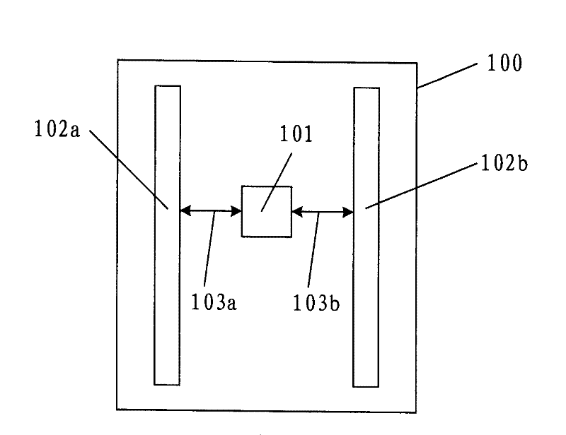
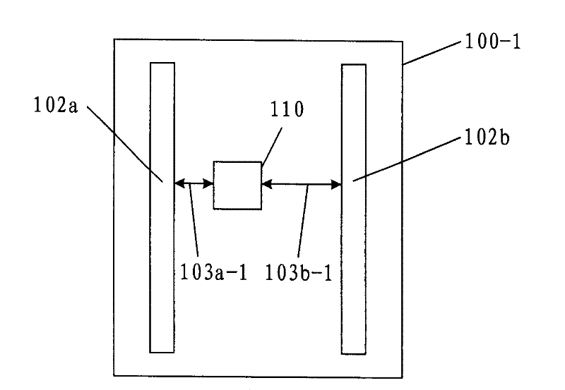
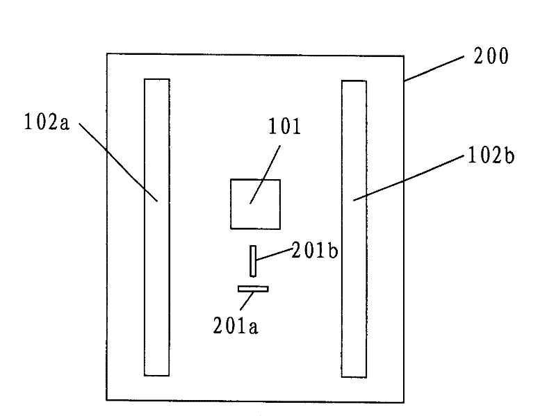
[0038] In order to make every defect on the reticle can be repaired, it is necessary to realize that any defects on the reticle can be accurately located. Existing masks have geometries that need to be transferred to the wafer surface during semiconductor fabrication. The geometry is determined by the l...


PUM


Abstract

The present invention discloses a mask plate, comprising a flat plate having light transmittance to exposure light, wherein, a printable geometric figure having light shading property to exposure light is formed on the flat plate; the geometric figure comprises at least one isolated figure; the isolated figure is provided with no other geometric figure or only the periodically repeated geometric figure along the X-axis and / or Y-axis direction in defect detection range. The present invention adopts a new layout design method, and is provided with the additional figure which cannot be printed in the detection range of the isolated figure in the geometric figure, so as to ensure that the defects of all positions can be positioned and repaired when defect repair is performed to the mask plate. Adopting the present invention can decrease the rejection rate of mask plates during mask plate manufacture and delay delivery risk.

Description

technical field [0001] The invention relates to the technical field of semiconductor manufacturing, in particular to a mask, a layout design method of the mask and a defect repair method. Background technique [0002] In the semiconductor manufacturing process, the lithography process is at the center and is the most important process step in the production of integrated circuits. The fabrication of semiconductor chips is usually divided into multiple layers, and the fabrication of each layer needs to be patterned to form specific structures, such as forming contact holes or metal wirings. The pattern definition of these specific structures is usually achieved by a photolithography process, which is a process that uses a photolithography mask to transfer the designed structure pattern to a wafer. [0003] Before the chip is fabricated, one or more photolithography masks are designed and fabricated according to the layout of devices, metal lines, connections, etc. on each la...

Claims


Application Information

Patent Timeline
Patent Type & Authority Patents(China)
IPC IPC(8): G03F7/14G06F17/50G03F1/00H01L21/00G03F1/72
Inventor 卢子轩
Owner SEMICON MFG INT (SHANGHAI) CORP
Why Eureka
Try Eureka