Shifting register as well as drive circuit and display device using said shifting register

A shift register and drive circuit technology, applied in static memory, digital memory information, instruments, etc., can solve the problems of drift, large leakage current, low mobility, etc., to reduce the number of clock pulse control signals, reduce complexity and area effect

Inactive Publication Date: 2008-06-18
CHUNGHWA PICTURE TUBES LTD
View PDF0 Cites 15 Cited by
  • Summary
  • Abstract
  • Description
  • Claims
  • Application Information

AI Technical Summary

Problems solved by technology

However, designing the driving circuit on the glass substrate of the liquid crystal display panel is easily limited by the poor characteristics of the transistor element, such as low mobility, threshold voltage shift, and large leakage current, etc... , so when designing the driving circuit on the liquid crystal display panel, it is necessary to select the components with special consideration of the above problems

Method used


Image

  • Shifting register as well as drive circuit and display device using said shifting register
  • Shifting register as well as drive circuit and display device using said shifting register
  • Shifting register as well as drive circuit and display device using said shifting register

Examples


Embodiment Construction

[0053] image 3 It is a circuit block diagram of a display device according to an embodiment of the present invention. Please refer to image 3 , the display device includes a display panel 301 , a clock controller 302 , a scan driving circuit 303 and a data driving circuit 304 . The display device in this embodiment is an example of a liquid crystal display device, and the scan driving circuit 303 is used as an example to illustrate the embodiment of the present invention.

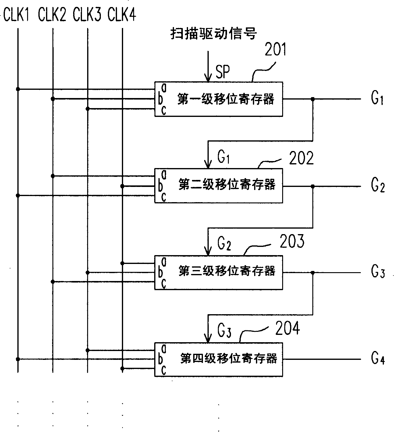
[0054] Figure 4 for the invention image 3 A circuit block diagram of the scan driving circuit 303 of the embodiment. Please refer to Figure 4 , the scan driving circuit 303 includes a plurality of shift registers 401 - 403 (here only three stages are shown as a representative). After the first-stage shift register 401 receives the scanning driving signal SP, it uses the control of the clock pulse signals CLK1~CLK3 to make the scanning driving signal SP sequentially output to the shift registers 4...


PUM


Abstract

The invention discloses a shift register and a driving circuit and a display device adopting the register. The shift register comprises a first commuting component and a second commuting component, and a first, second, third and fourth transistors. First source electrodes / drain electrodes of the first, second and third transistors respectively receive a common potential. Grids of the first and third transistors and a second source electrode / drain electrode of the second transistor are respectively coupled with a second terminal of the second commuting component. Grids of the second and fourth transistors and the second source electrode / drain electrode of the first transistor are respectively coupled with the second terminal of the first commuting component. The first source electrode / drain electrode of the fourth transistor is coupled with the second source electrode / drain electrode of the third transistor and the first terminal of the first commuting component receives input signals. A first terminal of the second commuting component receives a first clock impulse signal and a second source electrode / drain electrode of the fourth transistor receives a second clock impulse signal.

Description

technical field [0001] The present invention relates to a shift register, and in particular to a shift register which reduces the number of clock pulse control signals, a driving circuit and a display device using the shift register. Background technique [0002] At present, the thin-film transistor (TFT) used in most liquid crystal displays (LCD) is made of amorphous silicon (a-Si: H), so in large In the design of the liquid crystal display panel, a driving integrated circuit is added around the liquid crystal display panel. Use the gate voltage of the thin-film transistor to control the current between the source and the drain, turn the thin-film transistor on or off, and connect or disconnect it from the source of the driving signal at an appropriate time, so that each display pixel can operate independently, which is not easy Influenced by other display pixels. [0003] The driving circuit of the liquid crystal display, such as the scanning driving circuit and the data...

Claims


Application Information

Patent Timeline
IPC IPC(8): G11C19/28G09G3/36G02F1/13
Inventor 许峻源林展瑞魏湘云郭哲成黄俊尧
Owner CHUNGHWA PICTURE TUBES LTD
Why Eureka
Try Eureka