Digital transmission circuit and method providing selectable power consumption via multiple weighted drive slices

a digital transmission and drive slice technology, applied in the field of communication link circuits, can solve the problems of increasing the operating frequency and complexity of the interface between present-day system devices and between circuits, affecting the reliability of the signal transmission system, and consuming relatively large amounts of power budget of the integrated circuit, so as to reduce the area and complexity of the transmitter circuit and reduce the amount of control logi

a digital transmission and drive slice technology, applied in the field of communication link circuits, can solve the problems of increasing the operating frequency and complexity of the interface between present-day system devices and between circuits, affecting the reliability of the signal transmission system, and consuming relatively large amounts of power budget of the integrated circuit, so as to reduce the area and complexity of the transmitter circuit and reduce the amount of control logi

US7353007B2Active Publication Date: 2008-04-01INT BUSINESS MASCH CORP

Image

  • Digital transmission circuit and method providing selectable power consumption via multiple weighted drive slices
  • Digital transmission circuit and method providing selectable power consumption via multiple weighted drive slices
  • Digital transmission circuit and method providing selectable power consumption via multiple weighted drive slices

Examples


Embodiment Construction

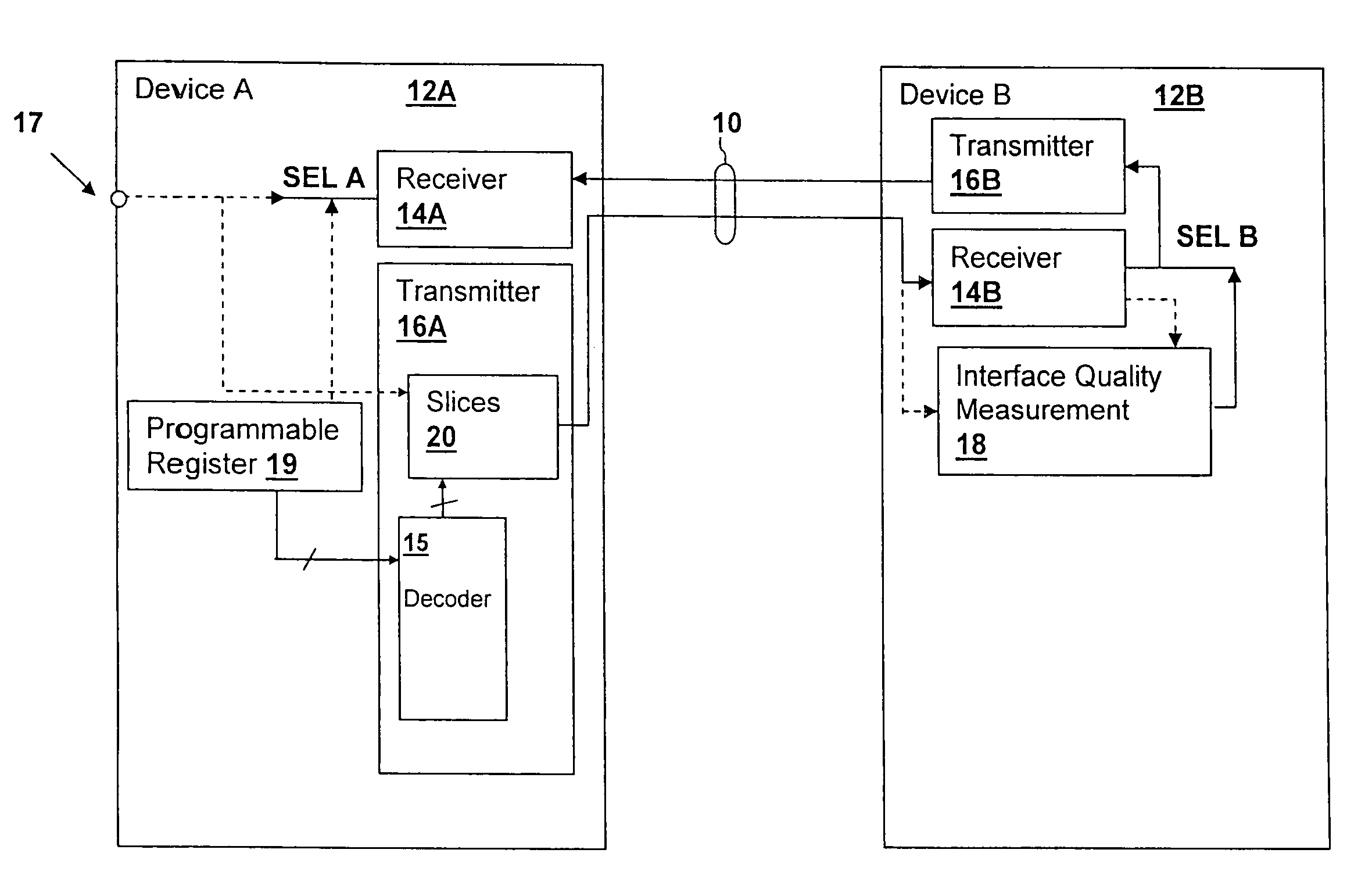
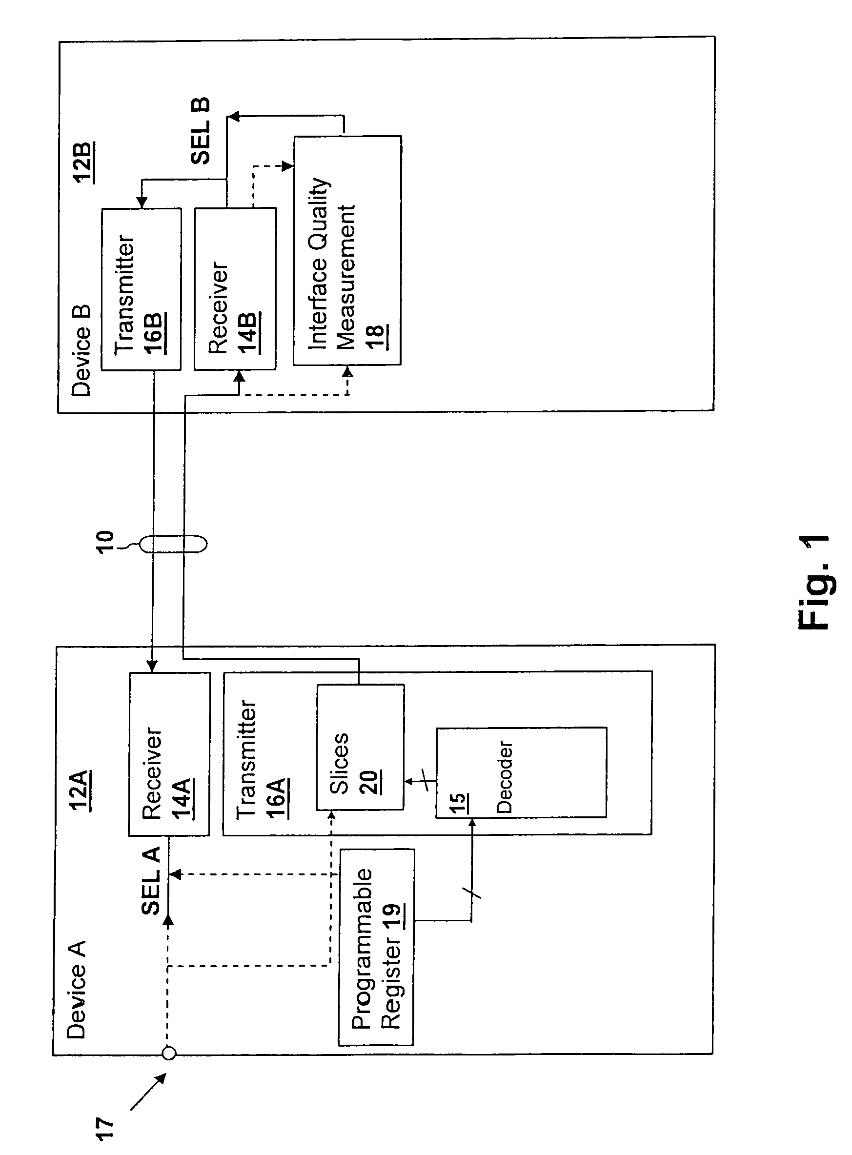
[0018]With reference now to the figures, and in particular with reference to FIG. 1, there is depicted a block diagram of transceivers 12A and 12B connected by an interface or channel 10 in accordance with an embodiment of the invention. Transceivers 12A, 12B may be located within a device such as a computer peripheral, a computer system, or within integrated circuits interconnected within a system. Interface 10 may be a single two wire bi-directional interface as depicted, or may be a full-duplex single wire interface or a bus having multiple transceivers in a half-duplex or full-duplex configuration. Transceivers 12A and 12B are connected to interface 10 each using a receiver 14A and 14B and a transmitter 16A and 16B, but the present invention is applicable to transmitters in general, and it should be understood that a transmitter in accordance with an embodiment of the invention may be incorporated in devices for connection to any of the above-specified types of interface 10, as ...


PUM


Abstract

A digital transmission circuit and method providing selectable power consumption via multiple weighted driver slices improves the flexibility of an interface while reducing transmitter power consumption, area and complexity when possible. A cascaded series of driver stages is provided by a set of parallel slices and a control logic that activates one or more of the slices, which combine to produce a cascaded active driver circuit. The power consumption / drive level selectability of the slice combination provides a driver that can be fine-tuned to particular applications to provide the required performance at a minimum power consumption level.

Description

CROSS-REFERENCE TO RELATED APPLICATIONS[0001]The present application is related to co-pending U.S. patent application Ser. No. 10 / 289,777, Publication No. 20040203483 entitled “INTERFACE TRANSCEIVER POWER MANAGEMENT METHOD AND APPARATUS”, filed on Nov. 7, 2002 and Ser. No. 10 / 829,829 entitled “METHOD AND SYSTEM FOR INTERACTIVE MODELING OF HIGH-LEVEL NETWORK PERFORMANCE WITH LOW-LEVEL LINK DESIGN”, filed on Apr. 22, 2004, both of said applications having at least one common inventor with, and assigned to the same assignee as, the present application. The specifications of the above-referenced Patent Applications are herein incorporated by reference.BACKGROUND OF THE INVENTION[0002]1. Technical Field[0003]The present invention relates generally to communication link circuits, and more particularly, to digital signal transmitters having selectable drive capability and power consumption.[0004]2. Description of the Related Art[0005]Interfaces between present-day system devices and betwee...

Claims


Application Information

Patent Timeline
01 Apr 2008
Publication
US7353007B2
IPC
H04B1/04
CPC
H04L25/0292; H04L25/028; H04L25/0272
Inventors
CARBALLO, JUAN-ANTONIO; NOWKA, KEVIN JOHN