LED lead frame and method for manufacturing LED using the lead frame

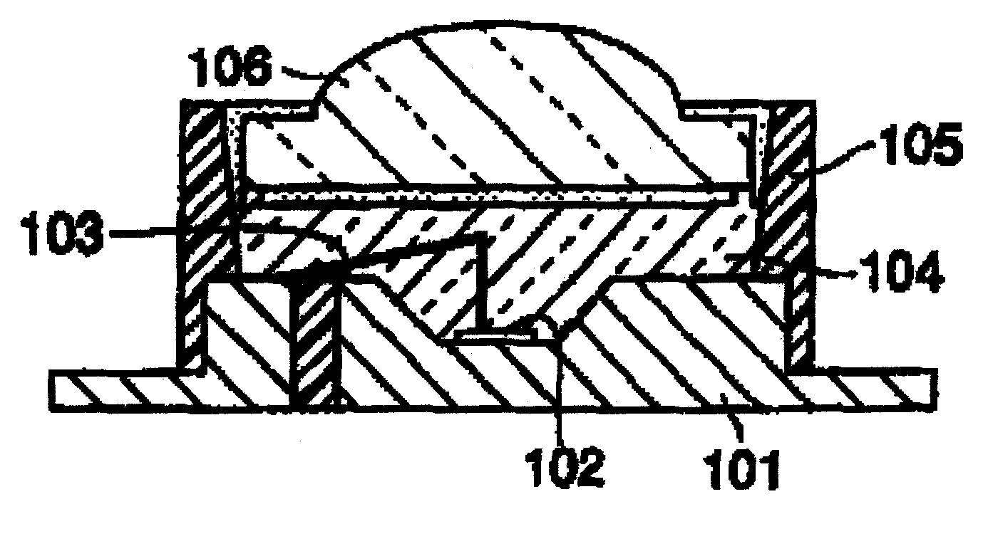
A lead frame and frame technology, applied in the direction of electrical components, electrical solid devices, circuits, etc., can solve the problem of delamination between the packaging colloid 104 and the reflective cavity 105, the difficulty of product consistency, and the inability to control heat dissipation and assembly density. Compare and other issues to achieve the effect of good product consistency, high production efficiency and high product reliability

Active Publication Date: 2010-09-22
FOSHAN NATIONSTAR OPTOELECTRONICS CO LTD
View PDF0 Cites 0 Cited by
  • Summary
  • Abstract
  • Description
  • Claims
  • Application Information

AI Technical Summary

Problems solved by technology

However, when used for a long time, especially for applications with harsh conditions such as outdoors, the phenomenon of delamination between the encapsulating colloid 104 and the reflective cavity 105 often occurs, thereby affecting the quality of the product, and this type of product is greatly restricted.
[0004] figure 2 It is a traditional bracket-type LED structure, which has the advantages of simple manufacturing process, but in the process of use, due to its own structural characteristics, it is often difficult to control the consistency of the final product, heat dissipation, assembly density and other characteristics Incomparable with SMD LED

Method used


Image

  • LED lead frame and method for manufacturing LED using the lead frame
  • LED lead frame and method for manufacturing LED using the lead frame
  • LED lead frame and method for manufacturing LED using the lead frame

Examples


Embodiment 1

[0030] Implementation example 1 provides a single-chip LED metal lead frame structure and a method for manufacturing LEDs using the lead frame:

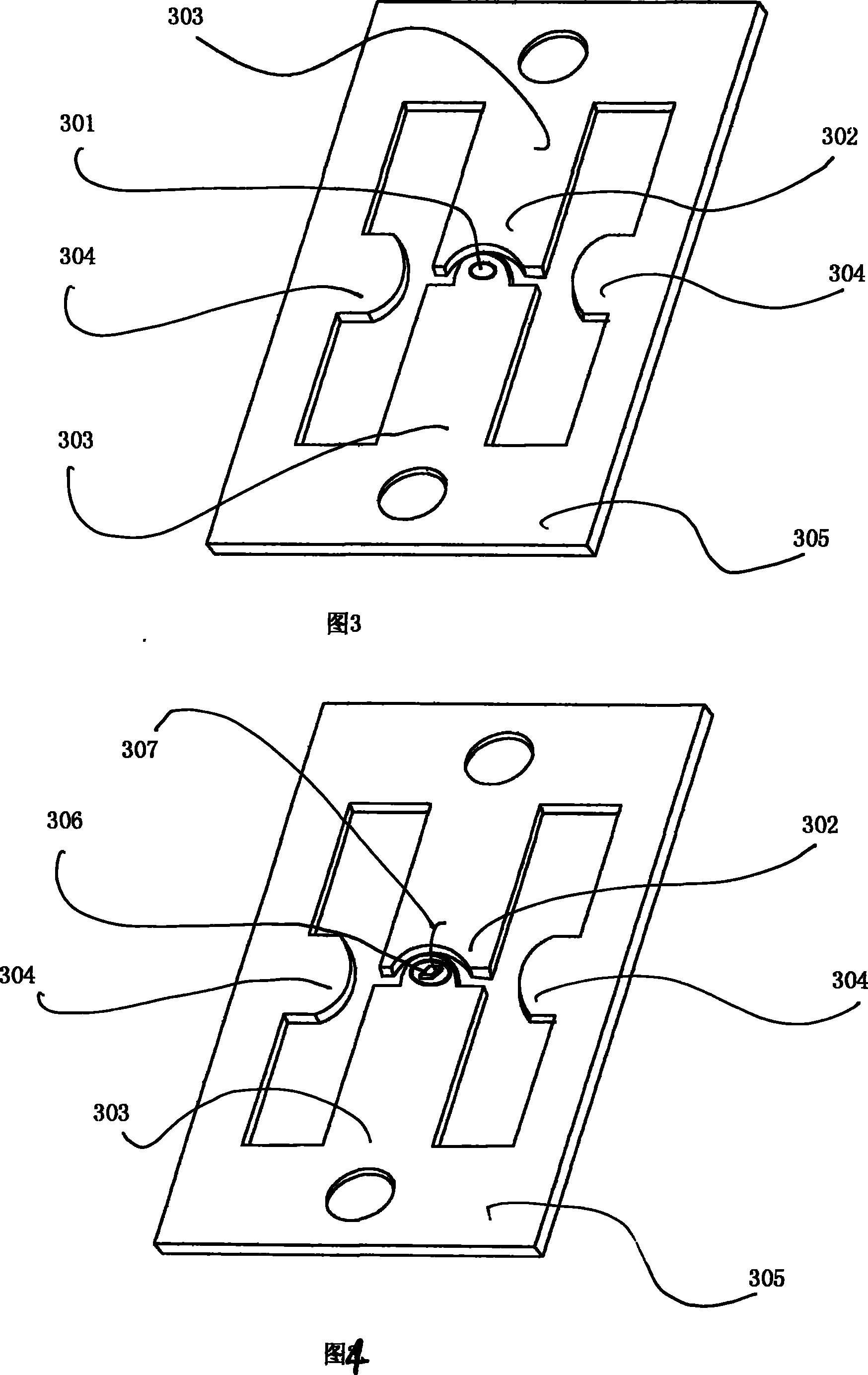
[0031] Such as image 3 The schematic diagram of the preforming of the metal lead frame is shown. The sheet metal plate frame structure with a thickness of 0.3mm is processed into a frame structure composed of convex plates extending toward the middle and spaced from each other in the peripheral frame. The peripheral frame constitutes a connecting substrate. The convex plates The metal lead frame that respectively constitutes several components of the chip placement part 301, the inner lead connection part 302, the outer electrode part 303, the tube body support part 304, and the connection substrate 305; The chip placement part and the chip placement part are located at the front end of the external electrode part, the chip placement part is provided with a reflection cavity, and the chip placement part 301 is provided with a reflec...

Embodiment 2

[0036] Implementation example 2 provides a solution for mass production of lead frames, which is an array structure of 4*10. Schematic such as Figure 8 shown.


PUM


Abstract

The invention discloses an LED lead frame, and the lead frame is a plate type frame structure. The invention is characterized in that a plate type frame is formed by arranging convex plates which are extended towards the middle part and mutually spaced in a peripheral frame, the convex plates respectively form a chip holding part, an inner lead connecting part, an outer electrode part and a pipe body supporting part, the peripheral frame forms a connecting base plate, the inner lead connecting part and the chip holding part are positioned at the front end of the outer electrode part, and the chip holding part is provided with a reflecting cavity. Simultaneously, the invention discloses a method for manufacturing an LED by adopting the lead frame, a process that encapsulating colloid is injected and moulded is adopted to cause the LED chip to be capsulated, and after a pin and an electrode outside the LED is punched and bent, the LED is separated from the base plate of the lead frame into an independent device. The invention has the advantages that the structure is simple, the LED lead frame is easy to be installed, and the consistency of the product is good.

Description

technical field [0001] The patent of the present invention relates to a light-emitting diode (LED) technology, in particular to a LED manufacturing technology, specifically a lead frame structure and a method for manufacturing an LED by using the lead frame. Background technique [0002] figure 1 and figure 2 Represents the known composition and structure diagram of LED, and respectively represents the two types of LED manufacturing methods commonly used at present [0003] figure 1 It is a PLCC type LED launched in recent years. This structure belongs to the surface mount type, and has the advantages of high assembly precision, high density, and high production efficiency. Its main components include lead frame 101, LED chip 102, connecting lead 103, encapsulation compound 104, reflective cavity 105, and lens 106. Lead wires 103 , and finally place the encapsulant 104 and the lens 106 . This type of LED generally has a reflective cavity 105 to facilitate the packaging...

Claims


Application Information

Patent Timeline
Patent Type & Authority Patents(China)
IPC IPC(8): H01L33/00H01L23/495H01L33/62
CPCH01L33/62H01L2224/48091H01L33/52H01L2224/45144
Inventor 余彬海李军政夏勋力缪来虎
Owner FOSHAN NATIONSTAR OPTOELECTRONICS CO LTD
Why Eureka
Try Eureka