
Liquid crystal display device

A liquid crystal display device and substrate technology, applied in nonlinear optics, instruments, optics, etc., can solve problems such as panel defects

Active Publication Date: 2008-07-02
JAPAN DISPLAY INC
View PDF1 Cites 7 Cited by
  • Summary
  • Abstract
  • Description
  • Claims
  • Application Information

AI Technical Summary

Problems solved by technology

Accompanied by this, there may be cases where the panel is defective due to static electricity from the outside of the panel due to factors such as the human body.

Method used


Image

  • Liquid crystal display device
  • Liquid crystal display device
  • Liquid crystal display device

Examples


Embodiment Construction

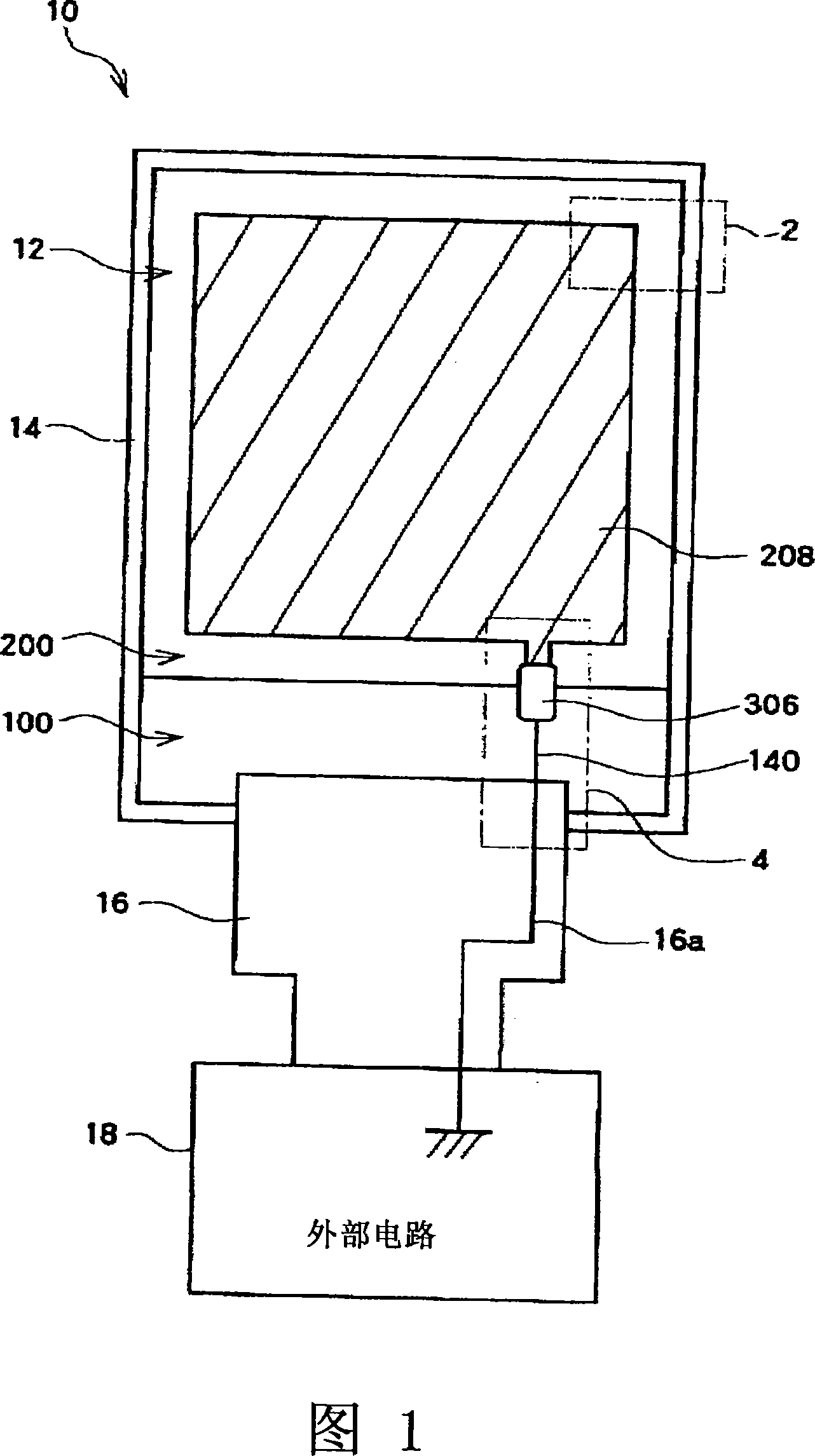
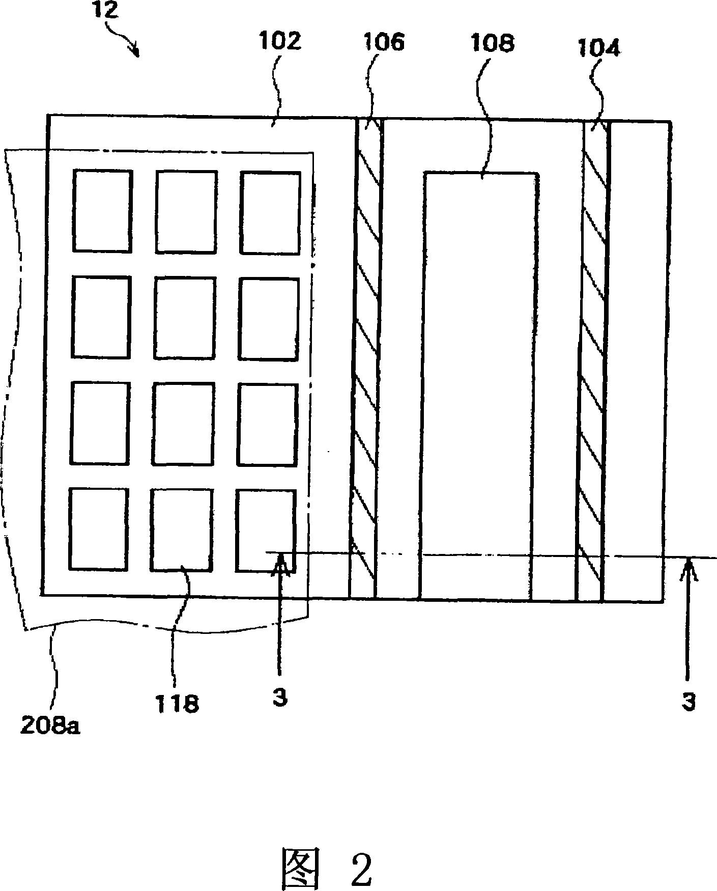
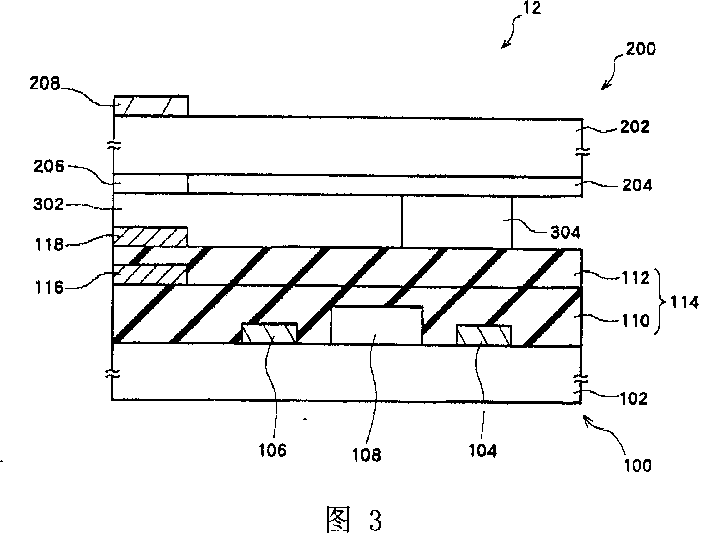
[0046] Before describing the embodiments of the present invention, various evaluations of the electrostatic withstand voltage characteristics have been considered. Therefore, for the antistatic characteristics considered, refer to the cross-sections near the peripheral portion of the liquid crystal display device shown in FIGS. 11 and 12. Figure to illustrate.

[0047] As shown in FIG. 11 and FIG. 12 , in the conventional liquid crystal display device 10Z in the FFS mode, the first substrate 100Z and the second substrate 200Z are bonded by a sealant 304Z, and these substrates 100Z, A liquid crystal 302Z is ​​sandwiched between 200Z. A circuit wiring group 104Z is arranged on a support substrate 102Z of the first substrate 100Z, and an insulating film 114Z is arranged to cover the circuit wiring group 104Z. In addition, in drawing, the circuit wiring group 104Z is shown schematically. On the outer surface of the supporting substrate 202Z of the second substrate 200Z, a light-...


PUM


Abstract

The present invention provides a liquid crystal display device, aiming at a liquid crystal display device in which a pixel electrode and a common electrode for driving a liquid crystal sandwiched between an opposing first substrate and a second substrate are arranged on the first substrate, Improves antistatic properties. The first substrate and the second substrate are arranged facing each other, and liquid crystal is sandwiched between the substrates. The pixel electrodes and common electrodes for driving liquid crystals are arranged on the first substrate. The first substrate includes circuit wiring arranged outside a pixel region where a plurality of pixels including pixel electrodes and common electrodes are arranged. The second substrate is provided with a light-transmitting conductive film disposed opposite to the pixel electrode and the common electrode and maintained at a predetermined potential on the side opposite to the liquid crystal, and the light-transmitting conductive film has a layer located on the second side of the second substrate than the outer edge of the second substrate. outer edge of the central side of the substrate.

Description

technical field [0001] The present invention relates to a liquid crystal display device, in particular to a device in which a pixel electrode and a common electrode for driving a liquid crystal sandwiched between a first substrate and a second substrate opposite to each other are provided on the first substrate. Liquid crystal display device. Background technique [0002] In the liquid crystal panel (liquid crystal panel) of FFS (Fringe Field Switching) mode, both the pixel electrodes (pixel electrodes) and the common electrodes for controlling the orientation of the liquid crystal are arranged on the element substrate, These two electrodes are stacked with an insulating film interposed therebetween. The upper electrode among the electrodes is provided with a slit. Rubbing is performed substantially parallel to the longitudinal direction of the slit, and when the potential between the electrodes is at an off potential, the liquid crystal molecules are aligned substantially...

Claims


Application Information

Patent Timeline
Patent Type & Authority Applications(China)
IPC IPC(8): G02F1/1333G02F1/1343
Inventor 青田雅明濑川泰生小野木智英
Owner JAPAN DISPLAY INC
Learn More