Crystal display device array substrate and driving method thereof

A technology for liquid crystal display devices and array substrates, which is applied in static indicators, nonlinear optics, instruments, etc., can solve problems such as increased energy consumption, high overall cost, and aging of liquid crystal pixel electrodes, so as to reduce usage and reduce overall costs. Effect

Inactive Publication Date: 2008-07-09
BOE TECH GRP CO LTD
View PDF0 Cites 98 Cited by
  • Summary
  • Abstract
  • Description
  • Claims
  • Application Information

AI Technical Summary

Problems solved by technology

[0004] But the main problem that exists in above-mentioned technology is: first, for TFT-LCD, the driving chip of control driving circuit includes scanning driving chip and data driver, all are indispensable, and the cost of driving chip is lower than TFT-LCD Occupy a large proportion in the production cost, and the data drive chip is more expensive than the scan driver because of its complex structure, making the overall cost of existing TFT-LCD products higher; The commonly used technical method is to invert the video data signal input by the data line, that is, invert the signal voltage, for example, set the common voltage in the common electrode to a constant value of 6V, and set the video data signal input by the data line to 0V ~12V, the voltage value

Method used


Image

  • Crystal display device array substrate and driving method thereof
  • Crystal display device array substrate and driving method thereof
  • Crystal display device array substrate and driving method thereof

Examples


Embodiment Construction

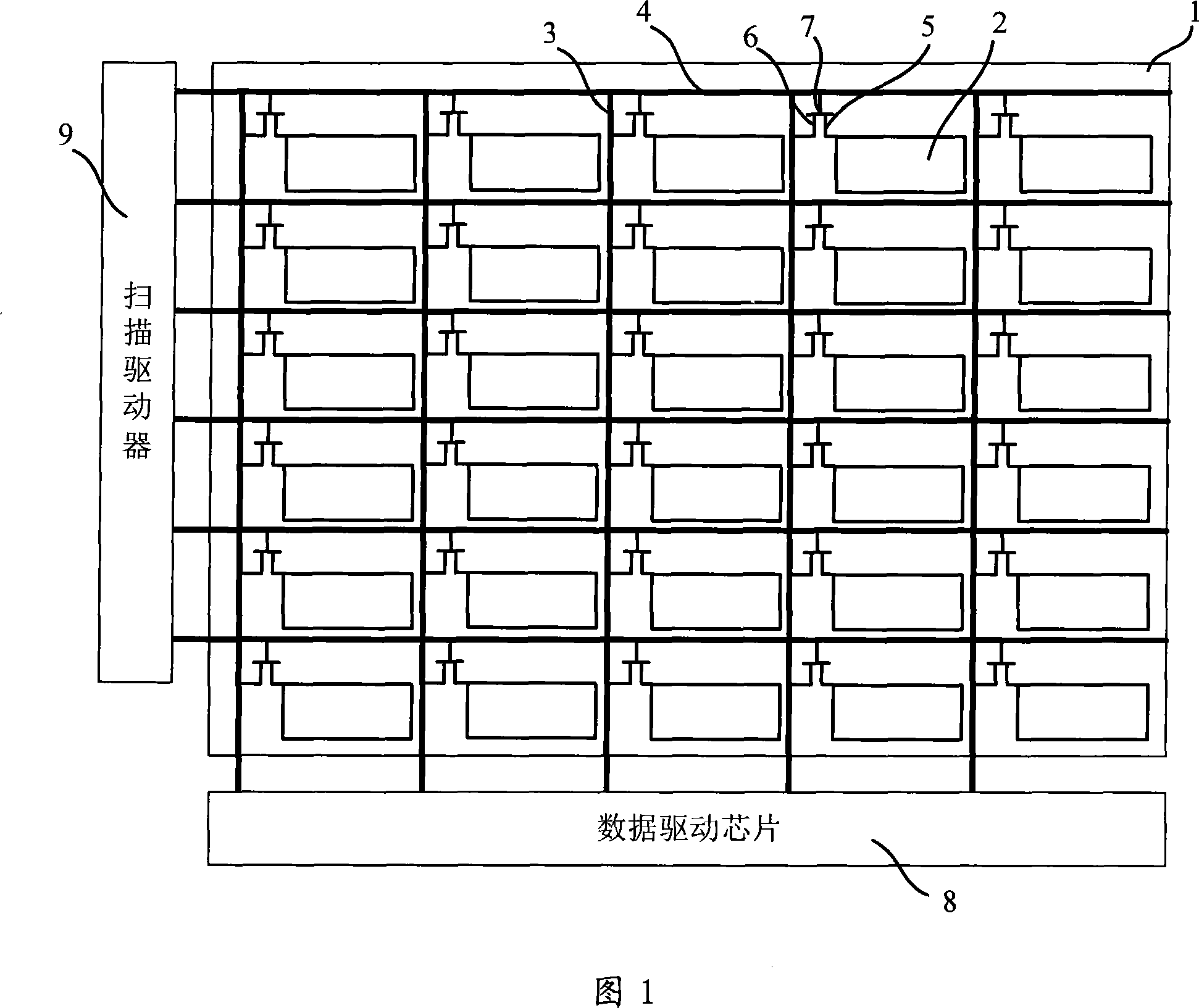
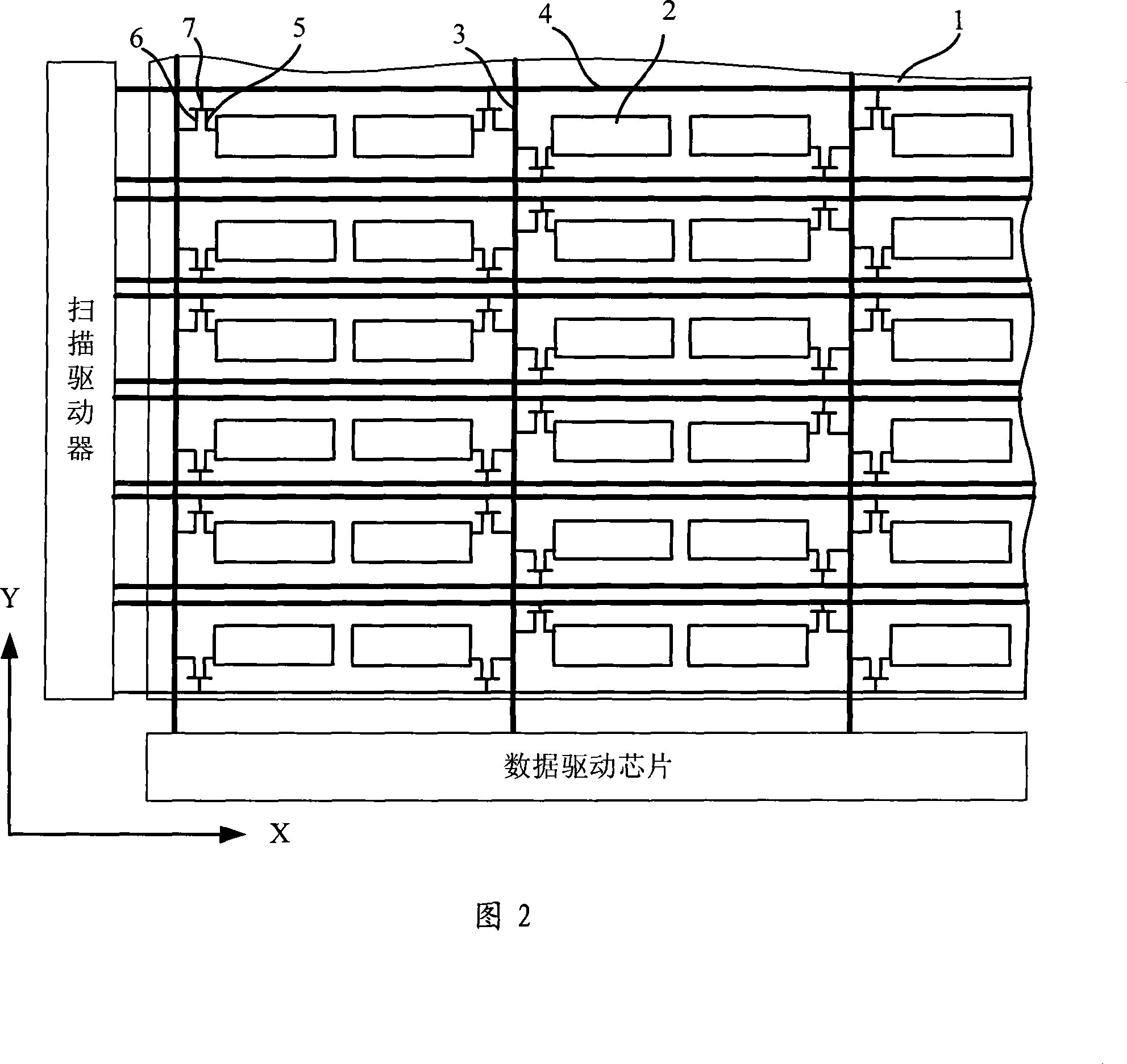
[0022] As shown in Figure 2, it is a structural schematic diagram of a specific embodiment 1 of the array substrate of the liquid crystal display device of the present invention. The array substrate of the liquid crystal display device includes: a base substrate 1, a liquid crystal pixel electrode, a data line 3 and a scanning line 4. It consists of three sub-pixel electrodes 2 arranged in a row. In FIG. 2, only a few local sub-pixel electrodes 2 of the array substrate of the liquid crystal display device are shown, wherein the sub-pixel electrodes 2 are arranged on the base substrate 1 in a matrix arrangement. Several parallel data lines 3 are arranged on the base substrate 1 longitudinally, that is, along the Y direction shown in FIG. on the bottom substrate 1. The relative positional relationship between the sub-pixel electrodes 2, the data lines 3 and the scanning lines 4 is specifically: each sub-pixel electrode 2 in the same column is connected to the same data line 3 ad...


PUM


Abstract

The invention relates to an LCD basal array and a driving method thereof. The basal array includes a substrate basal array, sub-pixel electrodes, datawires and scanning lines, which are in the same row. The sub-pixel electrodes in the same row are connected with one datawire and each datawire is connected with two rows of the sub-pixel electrodes. The sub-pixel electrodes in the same line are separately connected with the two scanning lines alternately in pairs and the sub-pixel electrodes connected with the same scanning line are positioned in the same line. Two sub-pixel electrodes in the same line between the two contiguous datawires are connected with the same scanning line and separately connected with the two datawires. The driving method includes the following steps of: inputting video data signals and sequentially driving the sub-pixel electrodes alternately connected with the two scanning lines in pairs via the two scanning lines when driving each row of the sub-pix electrodes. The invention uses the technical proposal that the two rows of sub-pixel electrodes share one datawire, thus greatly reducing the consumption of the required datawires and the data driving chips and the whole cost of the LCD device.

Description

technical field [0001] The invention relates to an array substrate of a liquid crystal display device and a driving method, in particular to an array substrate of a thin film transistor liquid crystal display device and a method for driving a driving circuit on the array substrate. Background technique [0002] Thin Film Transistor-Liquid Crystal Display (Thin Film Transistor-Liquid Crystal Display, hereinafter referred to as TFT-LCD) is one of the most widely used flat panel displays at present. TFT-LCD generally includes a liquid crystal display panel, a scan drive circuit and a data drive circuit. Wherein, the liquid crystal display panel includes a color filter substrate and a TFT array substrate arranged in opposite boxes, and a liquid crystal layer sandwiched between the two substrates, and a scanning driving circuit and a data driving circuit are respectively connected to the TFT switching elements on the array substrate. As shown in Figure 1, it is a schematic struc...

Claims


Application Information

Patent Timeline
IPC IPC(8): G02F1/1362G02F1/133G09G3/36
Inventor 张俊瑞邵喜斌尹海军
Owner BOE TECH GRP CO LTD
Why Eureka
Try Eureka