
Eureka
For R&D, Eureka makes reading and utilizing patents & technical documents easy.
Eureka AIR
Designed for self-driven R&D workflows. Generate viable solutions, solve complex R&D challenges, empower your innovation with AI.

Eureka Materials
Designed for material experts only. Revolutionize your material R&D, from search, analyze, to developing new materials.

TechResearch
Generate reliable direction feasibility study reports for your R&D in just a few steps.

TechSeek
Discover and master advanced knowledge NOW. Basics, ideas, possibilities, all at once.

TechMind
As an expert in R&D Theories, TechMind can generates customized viable solutions instantly.

TechRisk
Analyze your overall solution with one click, know your potential R&D risks in advance.

TechMonitor
Get weekly tech updates, stay abreast of the latest tech innovations and key insights.
Active matrix type display device and method for driving the same
An active matrix and display device technology, applied in static indicators, nonlinear optics, instruments, etc., can solve problems such as display unevenness, and achieve the effect of reducing display unevenness
- Summary
- Abstract
- Description
- Claims
- Application Information
AI Technical Summary
Problems solved by technology
Method used
Image

Examples
no. 1 Embodiment
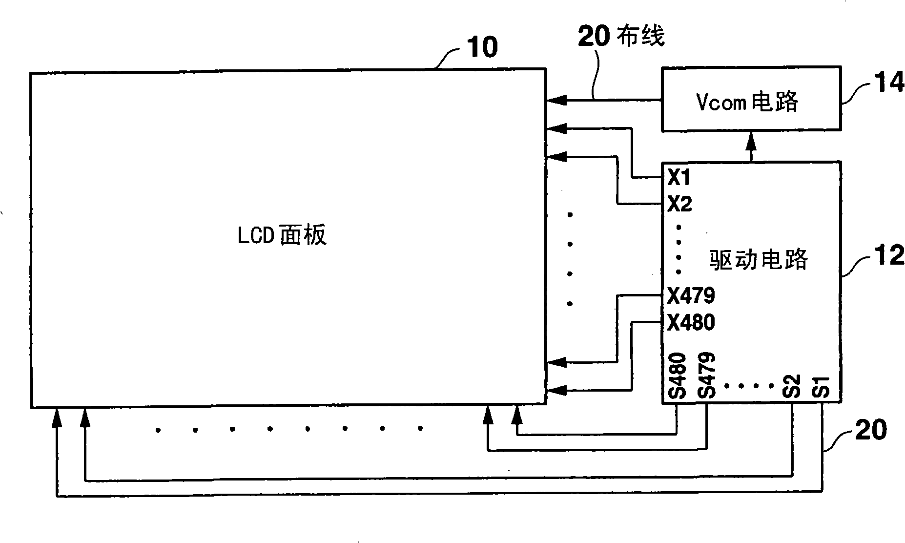
[0100] Figure 1A It is a schematic diagram showing the overall structure of the active matrix display device of the first embodiment of the present invention, Figure 1B for Figure 1A A schematic diagram of the pixel connection of the LCD panel in ;
[0101] That is, the active matrix type display device of this embodiment is like Figure 1A As shown, it is composed of a panel 10 provided with a plurality of pixel LCDs, a drive circuit 12 for driving and controlling each pixel of the LCD panel 10 , and a Vcom circuit 14 for applying a common voltage Vcom to the LCD panel 10 .
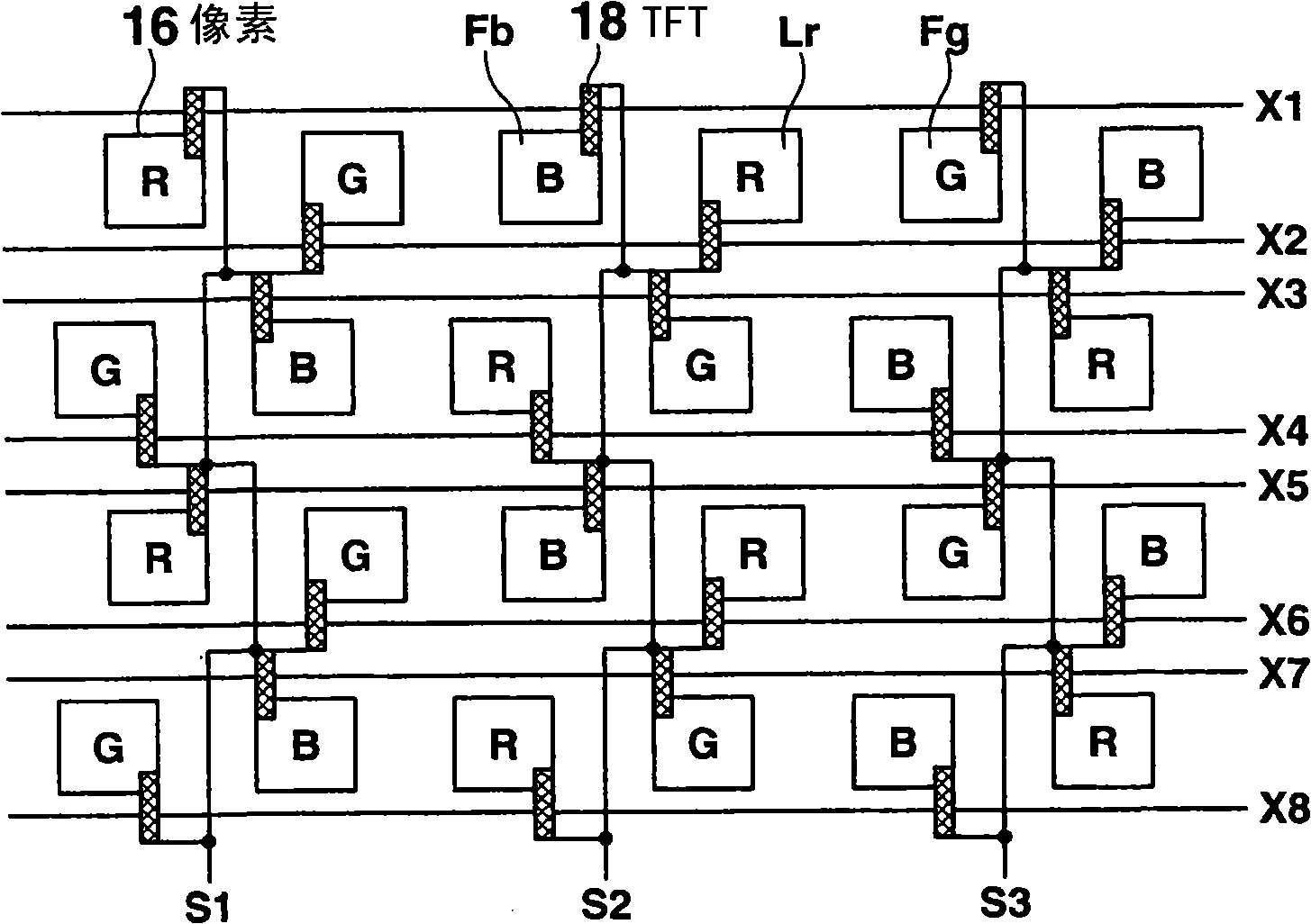
[0102] LCD panel 10 images Figure 1B As shown, a plurality of pixels are arranged in a matrix. In addition, a plurality of source lines S1 to S480 and a plurality of gate lines X1 to X480 are arranged to cross each other. In addition, each pixel is connected to one of the source lines and one of the gate lines through the TFT 18 which is a switching element. Here, each pixel is provided so that...
no. 2 Embodiment
[0146] Next, a second embodiment of the present invention will be described.
[0147] In this embodiment, the potential variation Vc caused by the inter-pixel parasitic capacitance Cpp is added to the previously written pixel potential and written, thereby canceling the potential variation Vc caused by the inter-pixel parasitic capacitance Cpp, and eliminating display failure. uniform.
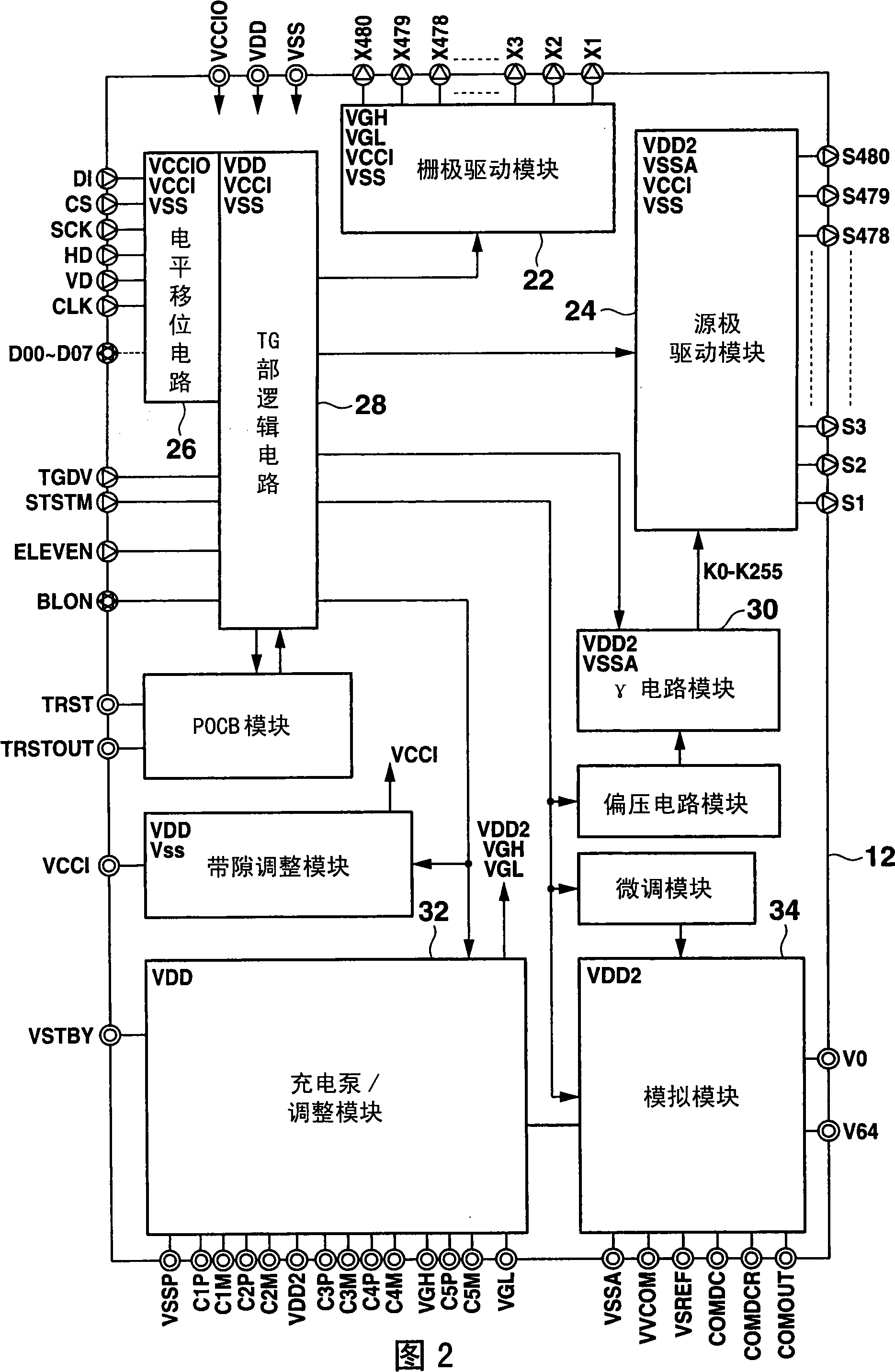
[0148] Here, a case where the potential variation is corrected using the gamma circuit module 30 of the drive circuit 12 will be described. In addition, the case of a still image in which unevenness tends to be conspicuous will be described.
[0149] As shown in FIG. 2 , the drive circuit 12 has a gamma circuit block 30 . Figure 5 It is a diagram showing the circuit configuration of the gamma circuit module 30 . As shown in the figure, the gamma circuit module 30 is composed of a gamma curve resistor 38 and a tap switch (hereinafter referred to as TAPSW) 40 . For the gamma curve resistor 3...
PUM
 Abstract
Description
Claims
Application Information
 - R&D Engineer
- R&D Manager
- IP Professional
- Industry Leading Data Capabilities
- Powerful AI technology
- Patent DNA Extraction
Browse by: Latest US Patents, China's latest patents, Technical Efficacy Thesaurus, Application Domain, Technology Topic, Popular Technical Reports.
© 2024 PatSnap. All rights reserved.Legal|Privacy policy|Modern Slavery Act Transparency Statement|Sitemap|About US| Contact US: help@patsnap.com