Method of preparing an integrated circuit die for imaging

A technology of integrated circuits and bare chips, which is applied in the field of inspection and analysis of integrated circuits, and can solve the problems of difficult extraction of circuit layout information and easy errors

Inactive Publication Date: 2008-10-15
CHIPWORKS INC
View PDF0 Cites 4 Cited by
  • Summary
  • Abstract
  • Description
  • Claims
  • Application Information

AI Technical Summary

Problems solved by technology

Circuit layout information is thus di

Method used


Image

  • Method of preparing an integrated circuit die for imaging
  • Method of preparing an integrated circuit die for imaging
  • Method of preparing an integrated circuit die for imaging

Examples


Embodiment Construction

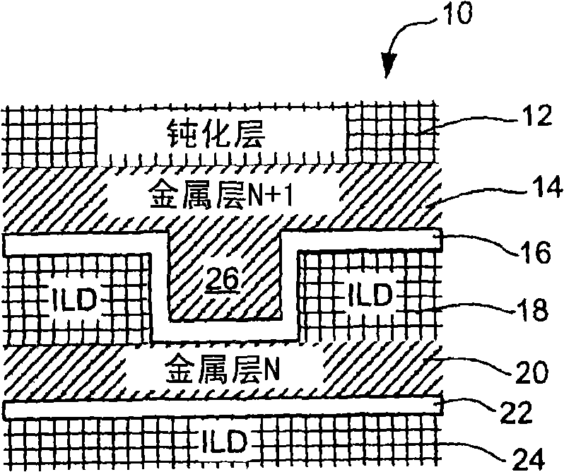
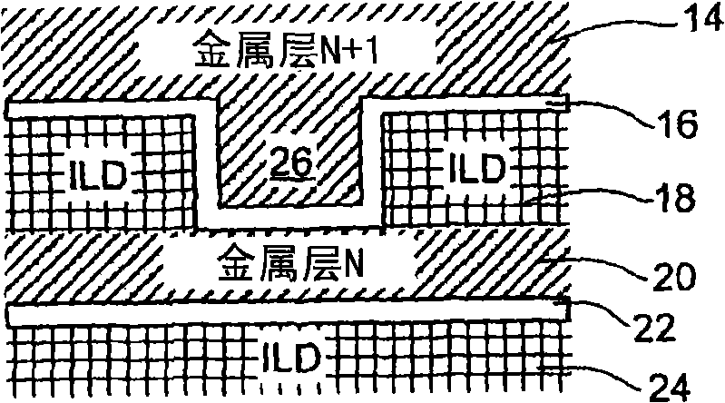
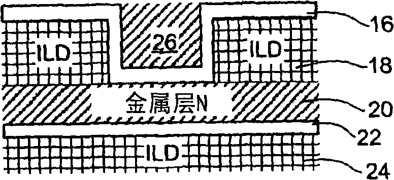
[0020] The present invention provides methods of preparing integrated circuit dies for imaging which are useful for preparing integrated circuit dies made by any process in which the metal lines and vias of the integrated circuit are formed with Made of the same metal. The method described above is very useful for integrated circuits made in an all-copper or all-aluminum process. However, the process is equally useful for making aluminum / tungsten integrated circuits traditionally used for imaging. According to the method described above, after exposing the metal layer of the integrated circuit, all the metal lines of the metal layer are etched away leaving the barrier layer material. When an image is taken with a scanning electron microscope, the barrier material appears in a first color, typically a light gray. If the chip is a copper / copper or aluminum / aluminum structure, the metal lines are etched away and the vias are also etched away, leaving a barrier layer surrounding...


PUM


Abstract

Integrated circuit dies are prepared for imaging by completely etching away all metal from the metal lines without removing barrier layers that underlie the metal lines. The metal vias may also be removed, especially if they are formed from the same metal as the metal lines, as in copper damascene circuits. This provides high contrast images that permits circuit layout extraction software to readily distinguish between metal lines and vias.

Description

technical field [0001] The present invention relates generally to inspection and analysis of integrated circuits and, more particularly, to methods of preparing integrated circuit dies for imaging to allow the structure and layout of integrated circuits to be extracted. Background technique [0002] As is well known in the art, inspection and analysis of integrated circuits requires sophisticated sample preparation techniques and imaging tools. In the past, integrated circuits were typically constructed using aluminum for the metal lines in each metal layer of the integrated circuit and tungsten for the vias that interconnect the metal lines, with the components formed on the polysilicon layer. Because aluminum and tungsten can be selectively etched, integrated circuits can be deconstructed using selective etching techniques that enable vias to be separated from metal lines, as will be described in more detail below with reference to FIG. 1 of. In addition, modern integrat...

Claims


Application Information

Patent Timeline
IPC IPC(8): G01R31/304G01R31/307
CPCG01R31/2898
Inventor 列夫・克利巴诺夫谢丽・林恩・格里芬
Owner CHIPWORKS INC
Why Eureka
Try Eureka