Method of manufacturing printed circuit board for semiconductor package

A printed circuit board and semiconductor technology, applied in the field of PCB manufacturing, can solve problems such as defects, weakening of electroplating gold process, and deterioration of wire bonding performance

Inactive Publication Date: 2008-10-22
SAMSUNG ELECTRO MECHANICS CO LTD
View PDF1 Cites 1 Cited by
  • Summary
  • Abstract
  • Description
  • Claims
  • Application Information

AI Technical Summary

Problems solved by technology

[0019] As described above, the method of manufacturing PCBs for semiconductor packaging according to the conventional technology is difficult because at least two or three masking operations are performed when two or three types of plating processes are performed, so that there is no Desirably, the gold plating process is prone to weakening due to penetration of masking fluid and defects due to residual plating resist
[0020] Also, in the case of electroless soft gold plating on the wire bonding pads, the wire problem may be solved, but the wire bonding performance may deteriorate accordingly
Also, the chemical soft gold plating process often results in poor SMD mounting reliability, while at least doubling the operating cost also makes it a problem

Method used


Image

  • Method of manufacturing printed circuit board for semiconductor package
  • Method of manufacturing printed circuit board for semiconductor package
  • Method of manufacturing printed circuit board for semiconductor package

Examples


Embodiment Construction

[0032] The present invention will be described in detail below with reference to the accompanying drawings.

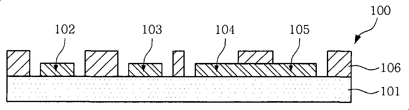
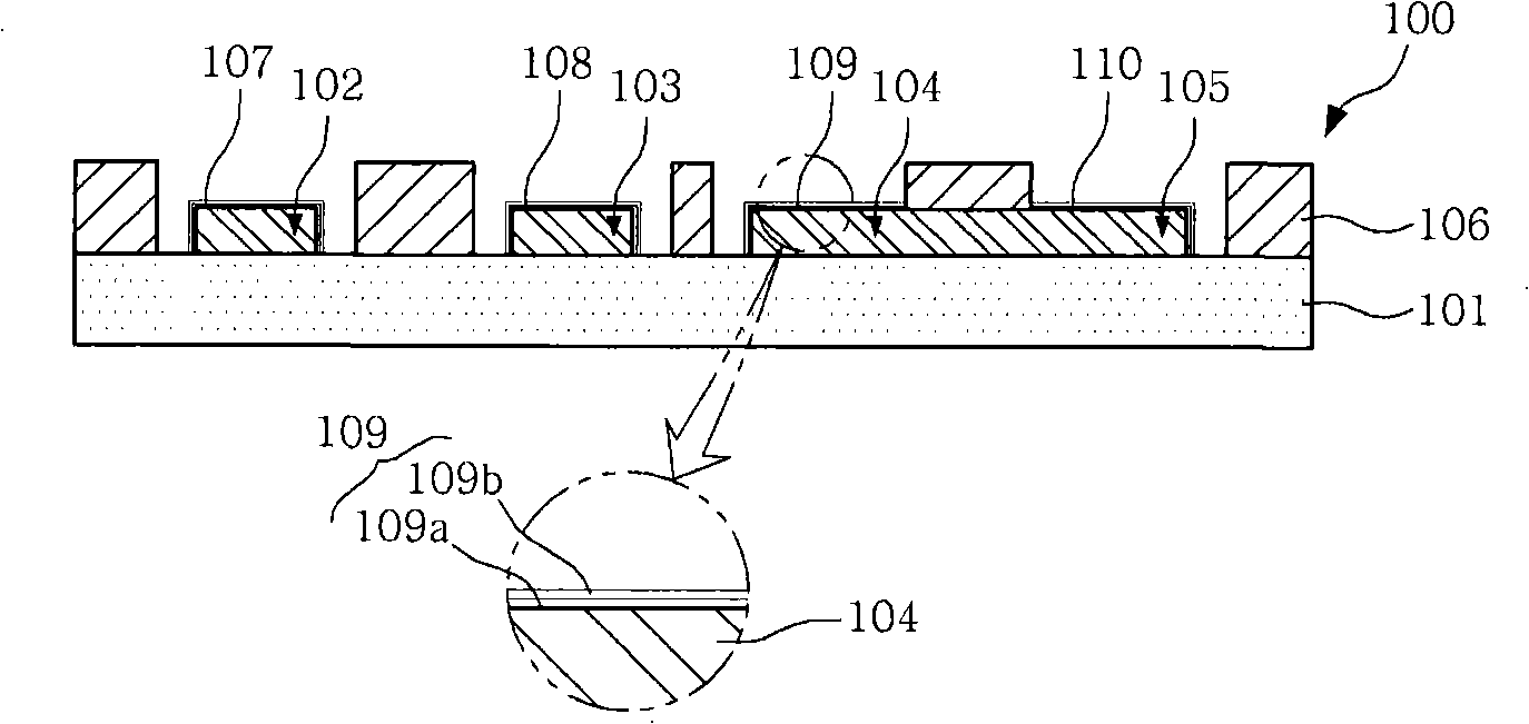
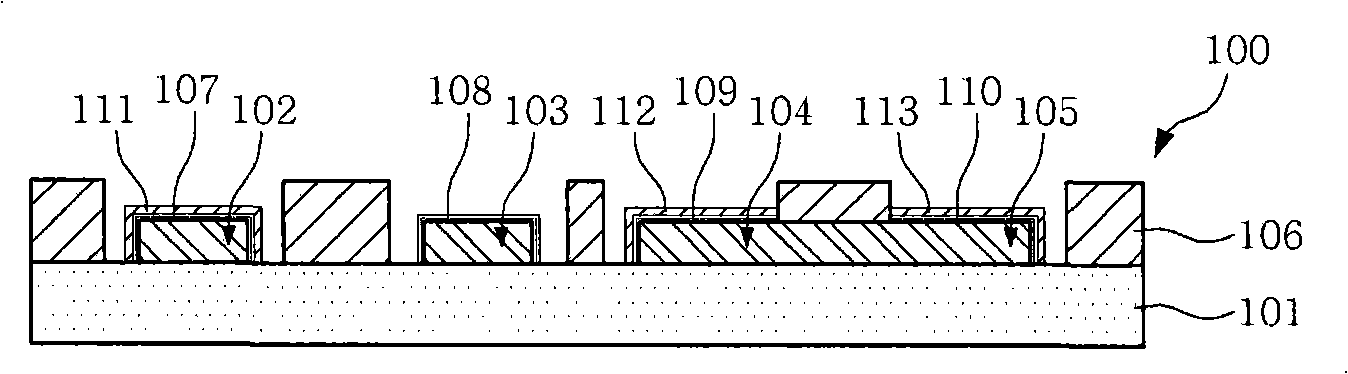
[0033] exist Figure 1A to Figure 1C In, a method for manufacturing a PCB for a semiconductor package according to a first embodiment of the present invention is schematically illustrated and described below.

[0034] According to a method well known in the art, a PCB 100 including a resin substrate 101, wire bonding pads 102, 105 and SMD mounting pads 103, 104 formed on the resin substrate and having a predetermined circuit pattern is prepared. In these figures, for simplicity of description, the inner layer structure of the substrate is omitted, and only a single side of the substrate is shown exemplarily, however any substrate, including double-sided, single-sided or multi-layer BGA or MLB substrates, may not be affected Applies to this limitedly. As with the resin substrate 101, any substrate including epoxy resin substrates, fluorinated resin substrates, and the...


PUM


Abstract

The invention discloses a production method of a printing circuit board of semiconductor capsulation. The invention enables that the masking work for plating each bonding pad in order to carry out surface treatment to the printing circuit board of semiconductor capsulation is reduced to the least or avoided completely, thereby simplifying total process and improving the reliability of installation.

Description

[0001] Related Application Cross Reference [0002] This application claims the benefit of Korean Patent Application No. 10-2007-0037892, filed Apr. 18, 2007, entitled "Method of Manufacturing Printed Circuit Board for Semiconductor Package," the disclosure of which is incorporated herein by reference in its entirety. technical field [0003] Generally, the present invention relates to a method of manufacturing a printed circuit board (PCB) for a semiconductor package. More particularly, the present invention relates to a method of manufacturing a PCB for a semiconductor package, which enables a mask to work when each pad is plated for surface treatment of the PCB for a semiconductor package minimized. Background technique [0004] In general, semiconductor packaging is a technology that has a significant impact on the proliferation of electronic hardware systems composed of active devices (such as semiconductor chips) and passive devices (such as resistors, capacitors, etc...

Claims


Application Information

Patent Timeline
Patent Type & Authority Applications(China)
IPC IPC(8): H01L21/48
CPCH05K2203/0723H01L2924/0002H05K2203/072H05K3/243H01L21/4846H05K3/244H05K2201/0391H01L2924/00H05K3/18
Inventor 李亮制金宏植安东基韩美贞许卿进林营奎
Owner SAMSUNG ELECTRO MECHANICS CO LTD
Why Eureka
Try Eureka