Semiconductor device and method for preventing attacks on the semiconductor device

A semiconductor and device technology, applied in the field of semiconductor devices, which can solve the problem of chip exposure to attacks

Inactive Publication Date: 2008-10-22
NXP BV
View PDF0 Cites 4 Cited by
  • Summary
  • Abstract
  • Description
  • Claims
  • Application Information

AI Technical Summary

Problems solved by technology

The drawback of this method is that the chip is expos

Method used


Image

  • Semiconductor device and method for preventing attacks on the semiconductor device
  • Semiconductor device and method for preventing attacks on the semiconductor device
  • Semiconductor device and method for preventing attacks on the semiconductor device

Examples


Embodiment Construction

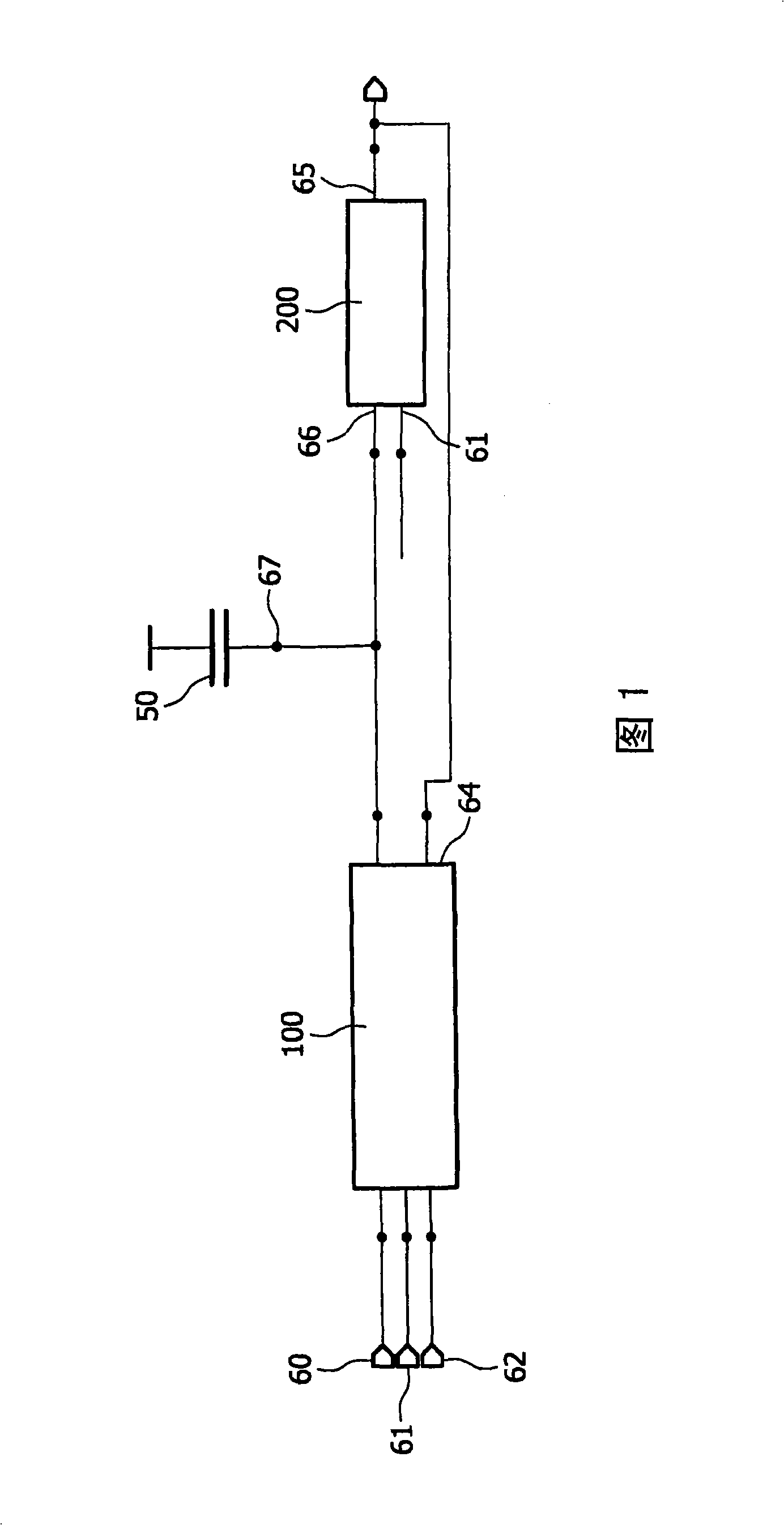
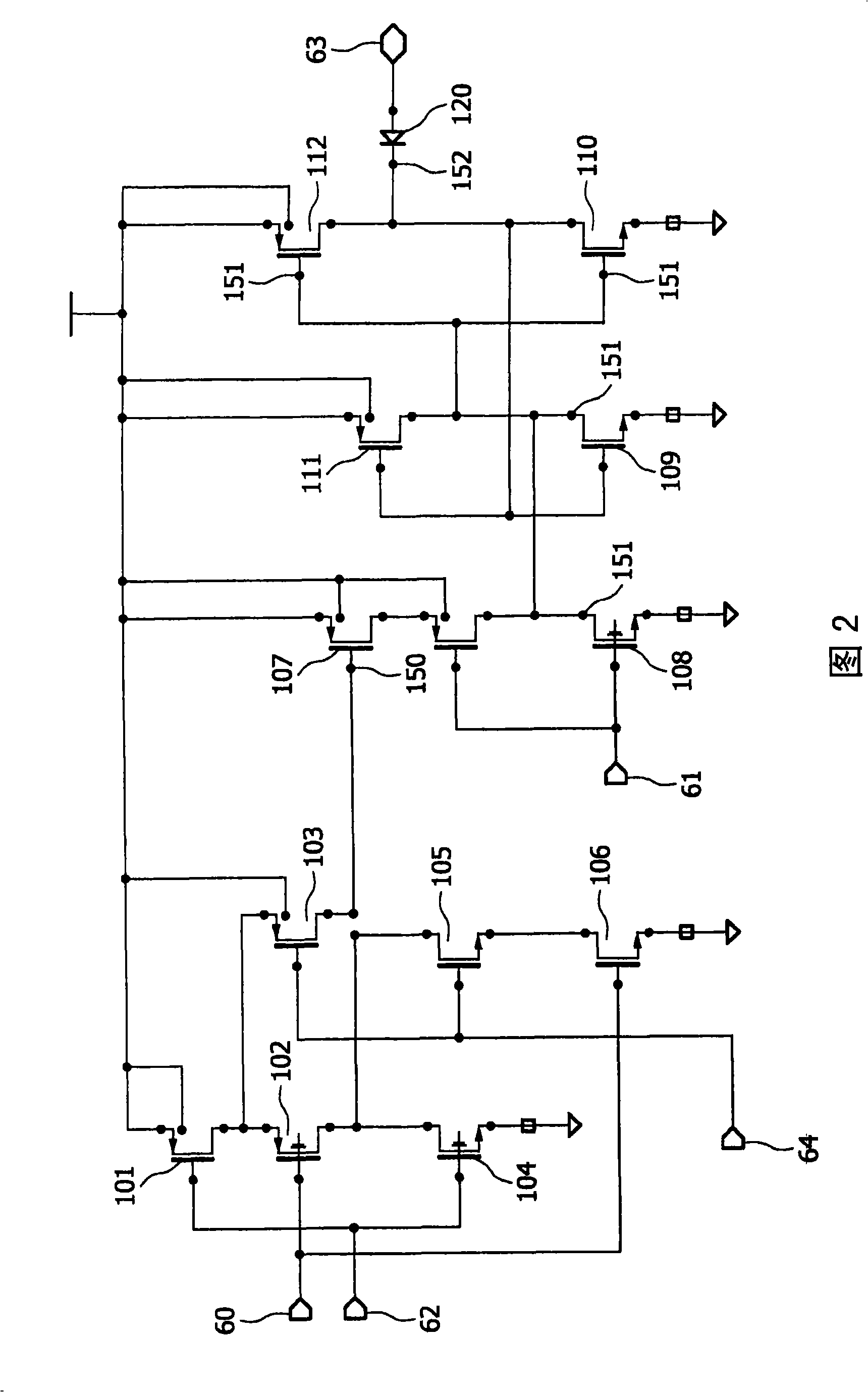
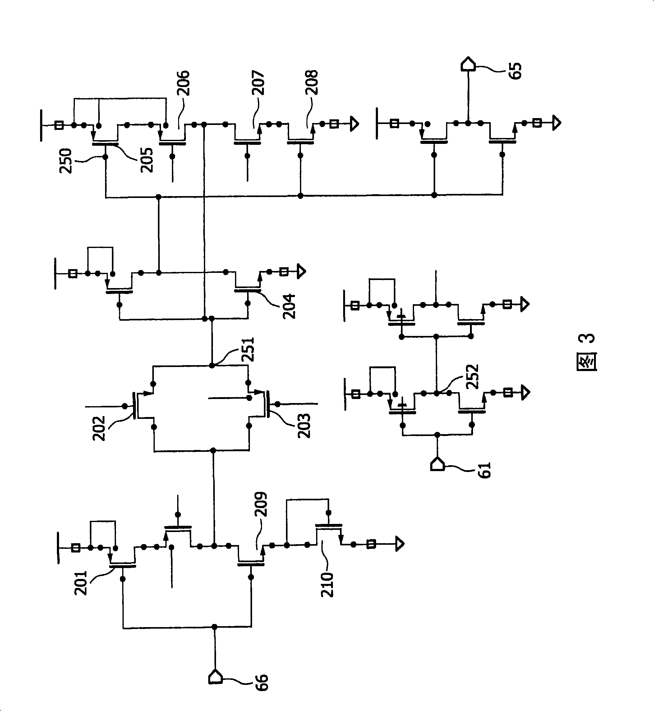
[0063]An example of an embodiment in which the semiconductor device is configured as a smart card chip is described below. The smart card chip includes means for storing items of information relating to the attack. An item of information may eg result from the reaction of one of the aforementioned sensors. The response of this sensor leads to initialization of the smart card chip. According to the invention, the items of information on the chip of the smart card which are relevant to the attack remain valid even after initialization. Once initialized, these items of information are read and used to trigger further initializations. This would cause the risk of an infinite loop of initialization, thereby preventing any update attack on the smart card chip.

[0064] If the smart card chip is disconnected from the supply voltage, the stored information items involved in the attack will remain intact for a predetermined period of time before being lost. Preferably, the time per...


PUM


Abstract

The invention relates to a method and to a semiconductor device, comprising means for detecting an unauthorized access to the semiconductor device, wherein the semiconductor device carries out an initialization of the semiconductor device following detection of an unauthorized access, wherein an information item relating to the unauthorized access can be stored by the semiconductor device prior to the initialization, and wherein the stored information item relating to the unauthorized access remains intact following the initialization of the semiconductor device. It is advantageously provided that the stored information item remains intact for a predetermined period of time following disconnection of the semiconductor device from a power supply.

Description

technical field [0001] The invention relates to a semiconductor device capable of initialization after being attacked and a corresponding method. Background technique [0002] Such a semiconductor device is used in particular as a chip of a smart card. Typically stored on the smart card chip are items of information intended to be obtained only by authorized persons. These items of information are, for example, secret information items for identifying the user or authorizing said user. The information items should not be accessible from the outside, since otherwise they could be misused. It is absolutely necessary to especially protect critical data which are used to encrypt items of information carried out externally. [0003] An attack on the safety or integrity of the product consists above all of exposing the chip to operating conditions outside of its specification, that is to say eg temperature, light, voltage, clock rate or voltage spikes applied to the chip. Ther...

Claims


Application Information

Patent Timeline
IPC IPC(8): G06F21/02G06F21/55G06F21/77
CPCG06F2221/2101G06F21/554G06F2221/2137G06F21/77G06F12/14G06F21/00
Inventor 约阿希姆·加尔贝森克·奥斯特敦
Owner NXP BV
Why Eureka
Try Eureka