Optical short distance amending method

An optical close-up, to-be-exposed technology, used in optics, originals for opto-mechanical processing, and photo-engraving processes for patterned surfaces, etc., can solve problems such as long time and achieve the effect of short time

Active Publication Date: 2008-10-29
SEMICON MFG INT (SHANGHAI) CORP
View PDF2 Cites 14 Cited by
  • Summary
  • Abstract
  • Description
  • Claims
  • Application Information

AI Technical Summary

Problems solved by technology

[0007] In the existing technology, it takes a long time to select the auxiliary graphics with the best distance from the circuit graphics, and generally takes 9 people x 24 hours / day x 1 month

Method used


Image

  • Optical short distance amending method
  • Optical short distance amending method
  • Optical short distance amending method

Examples


Embodiment Construction

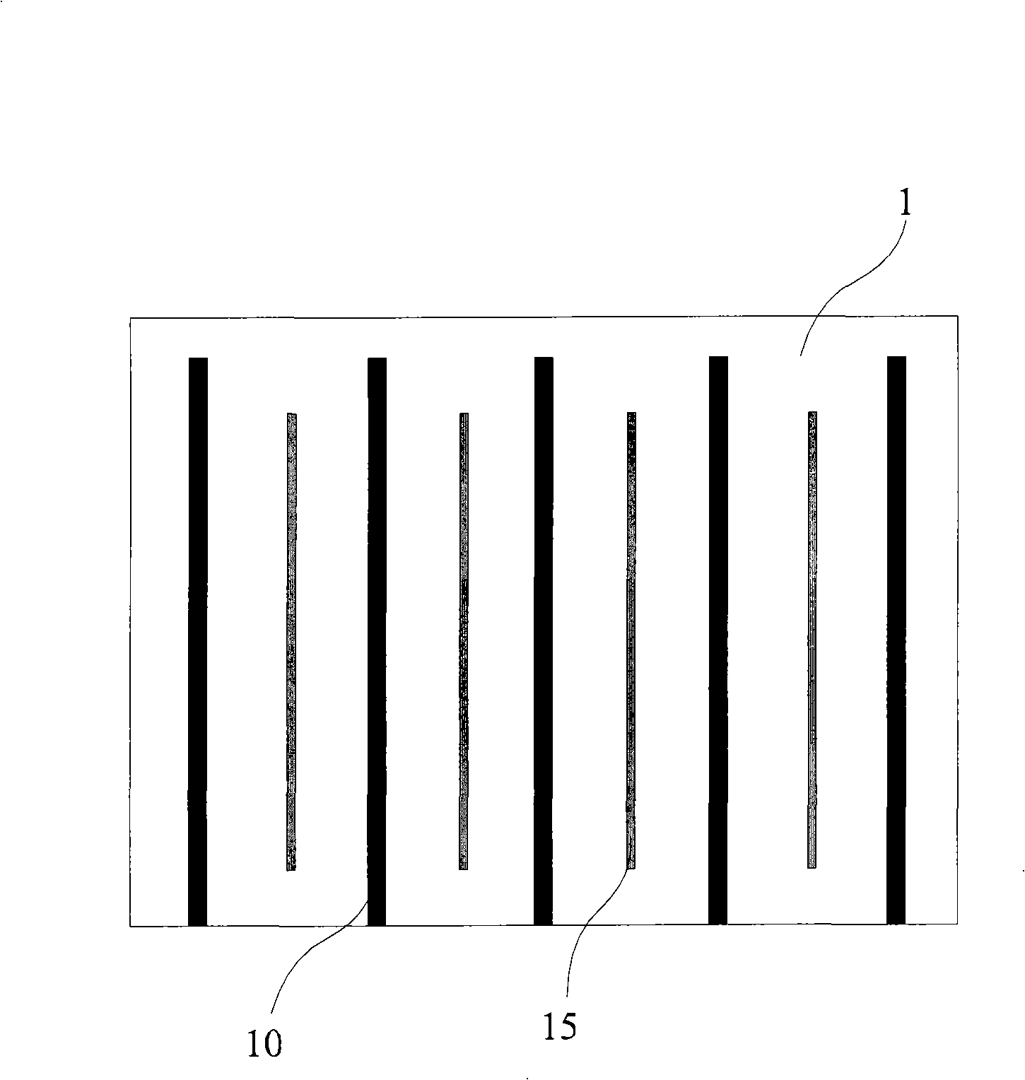
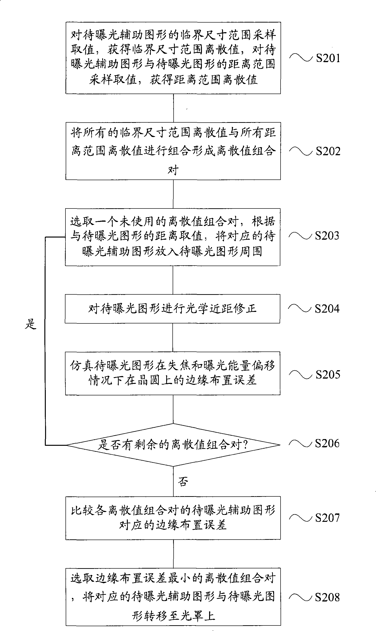
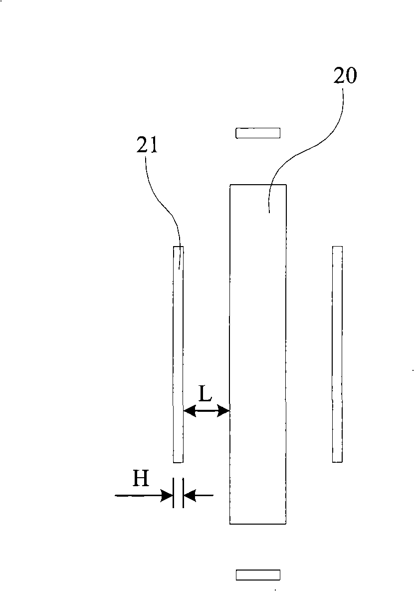
[0025] In the present invention, all the discrete values ​​of the critical size range within the critical size range of the auxiliary graphic to be exposed and the distance range from the graphic to be exposed are combined with all the discrete values ​​of the distance range to form a discrete value combination pair; an unused discrete value combination pair is selected , according to the value of the distance from the graphic to be exposed, put the corresponding auxiliary graphic to be exposed around the graphic to be exposed, perform optical short-distance correction and simulation, select the discrete value combination pair with the smallest edge layout error, and place the corresponding auxiliary graphic to be exposed The graphics and the graphics to be exposed are transferred to the mask. Since the auxiliary pattern to be exposed with the best distance from the pattern to be exposed and the optimal critical size is selected before making the mask, the time required for cor...


PUM

PropertyMeasurementUnit
critical dimensionaaaaaaaaaa

Abstract

The invention provides a method for optical close-distance correction, comprising the following steps of: sampling and getting value out of the critical dimension range of supporting graphics to be exposed and obtaining discrete values in the critical dimension range, sampling and getting value out of the distance range of the supporting graphics to be exposed and the graphics to be exposed and obtaining discrete values in distance range; combining all the discrete values in critical dimensional range with all the discrete values in distance range to form discrete value combination pairs; selecting the discrete value combination pairs, arranging corresponding supporting graphics to be exposed around the graphics to be exposed according to the distance values of the graphics to be exposed; carrying out the optical close-distance correction of the graphics to be exposed; simulating the edge arrangement errors of the graphics to be exposed on wafers under the situations of focus lost and exposal energy offset; selecting the discrete value combination pairs with the smallest edge arrangement errors, transferring the corresponding supporting graphics to be exposed and the graphics to be exposed to a photomask. By the steps, the time required by selecting the supporting graphics to be exposed which have the best distance and the best critical dimension with the graphics to be exposed is short.

Description

technical field [0001] The invention relates to the technical field of semiconductor manufacturing, in particular to an optical proximity correction (OPC, Optical Proximity Correction) method. Background technique [0002] With the rapid development of semiconductor manufacturing technology, in order to achieve faster computing speed, larger data storage capacity and more functions of semiconductor devices, semiconductor chips are developing towards higher integration; and the higher the integration of semiconductor chips, The critical dimension (CD, Critical Dimension) of the semiconductor device is smaller. Under the condition of 90nm process, the CD of VLSI application has entered the range of tens to hundreds of nanometers. [0003] In order to achieve tiny CDs, a finer image on the photomask must be focused on the photoresist of the semiconductor substrate, and the optical resolution must be increased to fabricate semiconductor devices approaching the optical resolutio...

Claims


Application Information

Patent Timeline
Patent Type & Authority Applications(China)
IPC IPC(8): G03F1/14G03F1/36
Inventor 刘庆炜
Owner SEMICON MFG INT (SHANGHAI) CORP
Why Eureka
Try Eureka