Electronic parts packages and method for forming a cavity thereof

An electronic component and cavity technology, which is applied in the field of electronic component packaging and the cavity forming the electronic component package, can solve the problems of reduced degrees of freedom, difficulty in controlling azimuth angle and brightness, etc., and achieve simple control, simple azimuth angle and brightness. Effect

Inactive Publication Date: 2008-12-10
阿莫卢克斯有限公司
View PDF0 Cites 12 Cited by
  • Summary
  • Abstract
  • Description
  • Claims
  • Application Information

AI Technical Summary

Problems solved by technology

However, in the LED package of Fig. 3, since the oblique sides of the cavity are flat, the degree of freedom is reduced
Therefore, it is difficult to control various azimuths and brightness

Method used


Image

  • Electronic parts packages and method for forming a cavity thereof
  • Electronic parts packages and method for forming a cavity thereof
  • Electronic parts packages and method for forming a cavity thereof

Examples


Embodiment Construction

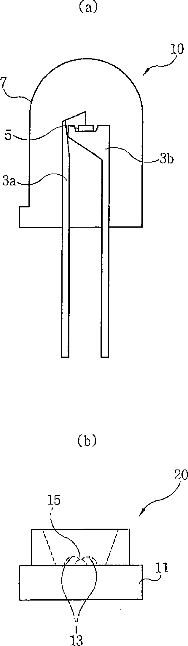
[0061] Hereinafter, an electronic component package according to the present invention and a method of forming a cavity of the electronic component package will be described with reference to the accompanying drawings. Hereinafter, a semiconductor package (ie, LED package) to which a light emitting diode is applied as an electronic component package will be described.

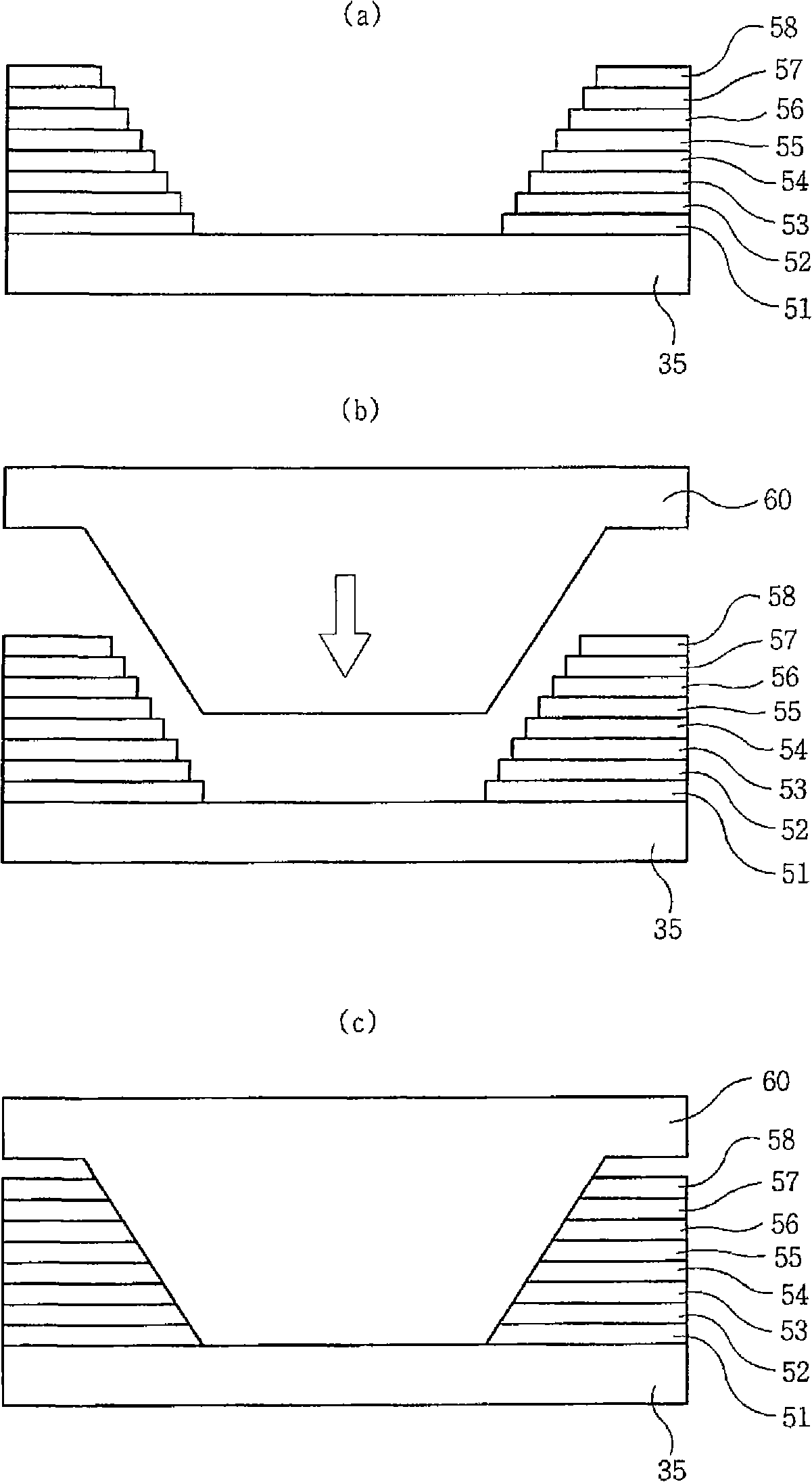
[0062] Figure 6 Is a cross-sectional view of the electronic component package according to the first embodiment of the present invention;

[0063] Figure 6 The LED package is configured with: a chip-type LED device 62; a lower ceramic substrate 60 on which the LED device 62 will be mounted; an upper ceramic substrate 70 arranged on the lower ceramic substrate 60, in the upper ceramic substrate 70, in the position A cavity having a predetermined shape is formed in an area corresponding to the area on which the LED device 62 will be mounted; pattern electrodes 64 and 66 formed on the lower ceramic substrate 60; a...


PUM


Abstract

Disclosed is an electronic part package for improving reflectability of light emitted from a light emitting device, and a method of forming a cavity of the electronic part package to improve the reflectability of light so that the cavity of a ceramic substrate is easily formed to have the desired shape. The cavity of the ceramic substrate has a shape tapered inward so that an inclined side is roundly concave and convex. The method includes shifting a tool that includes a cutting part having a cutting blade formed on an external surface thereof toward the ceramic substrate by a predetermined distance while the tool rotates along with a rotational processing part of a ceramic processing device and returning the tool to an original position of the tool to form a cavity having the inclined side in the ceramic substrate.

Description

Technical field [0001] The invention relates to an electronic component package and a method of forming a cavity of the electronic component package. More specifically, the present invention relates to an electronic component package that maximizes the luminous efficiency of light emitted from a light emitting device and a method of forming a cavity in a ceramic substrate of the electronic component package through a simple process. Background technique [0002] Light-emitting diodes (hereinafter referred to as LEDs) are semiconductor devices that can provide various colors. The LED contains a light emitting source, which is provided to change compound semiconductor materials such as GaAs, AlGaAs, GaN, InGaN, and AlGaInP. Currently, packaged semiconductor devices are applied to electronic parts. [0003] Generally, the standard for determining the performance of LED devices is the range of color, brightness, and luminous intensity. The performance of the LED device is determined ...

Claims


Application Information

Patent Timeline
Patent Type & Authority Applications(China)
IPC IPC(8): H01L33/00H01L33/46H01L33/48H01L33/64
CPCH01L33/483H01L33/46H01L33/60H01L2224/48091H01L2224/49107
Inventor 李永一朴淙远赵允旻
Owner 阿莫卢克斯有限公司
Why Eureka
Try Eureka