Device for connecting processor and BOOT FLASH and implementing method

A technology for connecting devices and processors, applied in electrical digital data processing, instruments, etc., can solve problems such as high cost, unfavorable implementation, changing byte order, etc., and achieve the effect of low cost and simple method

Inactive Publication Date: 2010-06-16
GLOBAL INNOVATION AGGREGATORS LLC
View PDF7 Cites 0 Cited by
  • Summary
  • Abstract
  • Description
  • Claims
  • Application Information

AI Technical Summary

Problems solved by technology

However, when the memory uses BOOT FLASH, the byte order cannot be changed by software, which brings great risks to hardware design.
[0010] The Chinese patent application number 200410030047.9 discloses a data sharing device and a processor for sharing data between processors with different byte sequences. The realization of this invention is mainly based on the conversion of the data address of the processor. When BOOT FLASH cannot change the byte order by software, but the processor needs to be greatly improved, which consumes a large cost and is not conducive to the implementation

Method used


Image

  • Device for connecting processor and BOOT FLASH and implementing method
  • Device for connecting processor and BOOT FLASH and implementing method
  • Device for connecting processor and BOOT FLASH and implementing method

Examples


Embodiment Construction

[0032] The present invention will be described in further detail below in conjunction with accompanying drawing and specific embodiment:

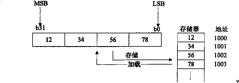
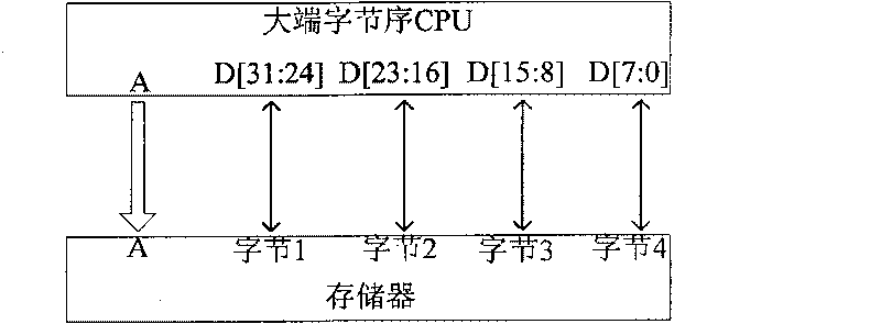
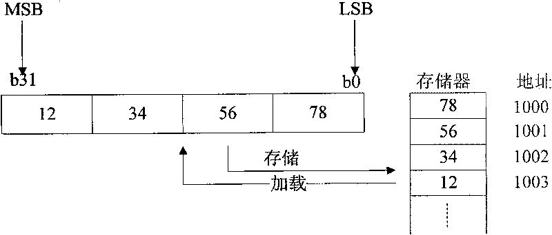
[0033] see Figure 5 , this figure is a schematic diagram of the connection between the CPU and the memory using the connection device of the present invention, wherein the connection device is a programmable logic device, which is a ROM type PLD device; the memory is BOOT FLASH, and the industry BOOT FLASH usually samples 8 or 16 bits The NOR FLASH of data bus width, because the situation of 8-bit data bus does not have the problem of byte order, so the present invention only needs to consider the situation of 16-bit data bus width; CPU can make big-endian byte order, also can be little-endian byte order.

[0034] During the application process, the connection device is fixedly connected to the bus interfaces of the CPU and the memory respectively, wherein the connection device and the data bus of the CPU adopt a default connection mode (...


PUM


Abstract

The invention discloses a connecting device between a processor and a BOOT FLASH, and a realization method thereof. The connecting device comprises a bus logic processing unit, a controlling unit anda startup register; the startup register is used for storing the start identification of the BOOT FLASH; the controlling unit is used for monitoring the start identification and determines whether theBOOT FLASH is started successfully or not, and if so, a control signal for directly transmitting a bus signal is sent to the bus logic processing unit; and if not, a control signal which performs reversal processing to the data bus signal in the bus according to the byte order and then transmits the data bus signal is sent to the bus logic processing unit; the bus logic processing unit is connected with the processor in a default connection manner, and the corresponding connection manner can also be adopted for connection according to the byte order of the BOOT FLASH. The dynamic selection ofthe connection manner of the byte orders between the CPU with different byte orders and the BOOT FLASH can be realized, the method is simple, and the cost is lower.

Description

technical field [0001] The invention relates to a connection device between processors with different byte sequences and BOOT FLASH (boot flash memory) and its realization method. Background technique [0002] In the field of embedded system design, regardless of hardware design or software design, byte order is a problem that must be considered. The so-called byte order is the order of bytes, which is the access order of data larger than one byte in the memory. There are two ways: big endian and little endian. . [0003] Big-endian is the way in which bytes are arranged when storing more than two bytes of data in a memory with a byte-unit address. At this time, the byte of the big-endian MSB is stored in ascending order of the address of the memory. Endianness is the order in which bytes are arranged, not bits, and the order in which bits are arranged within a byte does not change. [0004] figure 1 An illustration showing big-endian byte ordering. As shown in the figu...

Claims


Application Information

Patent Timeline
Patent Type & Authority Patents(China)
IPC IPC(8): G06F13/16
Inventor 王凤彬
Owner GLOBAL INNOVATION AGGREGATORS LLC
Why Eureka
Try Eureka