Thin film transistor manufacturing method, thin film transistor and display device using the same

A technology of thin film transistors and manufacturing methods, applied in the direction of transistors, semiconductor/solid-state device manufacturing, electric solid-state devices, etc., can solve problems such as L length deviation, and achieve the effect of excellent image quality

Inactive Publication Date: 2008-12-24
SONY CORP
View PDF5 Cites 8 Cited by
  • Summary
  • Abstract
  • Description
  • Claims
  • Application Information

AI Technical Summary

Problems solved by technology

Therefore, the problem caused by the deviation of the length of L remains to be solved

Method used


Image

  • Thin film transistor manufacturing method, thin film transistor and display device using the same
  • Thin film transistor manufacturing method, thin film transistor and display device using the same
  • Thin film transistor manufacturing method, thin film transistor and display device using the same

Examples


Embodiment Construction

[0025] The thin film transistor manufacturing method, the thin film transistor and the display using the thin film transistor according to the present invention will be described below with reference to the accompanying drawings.

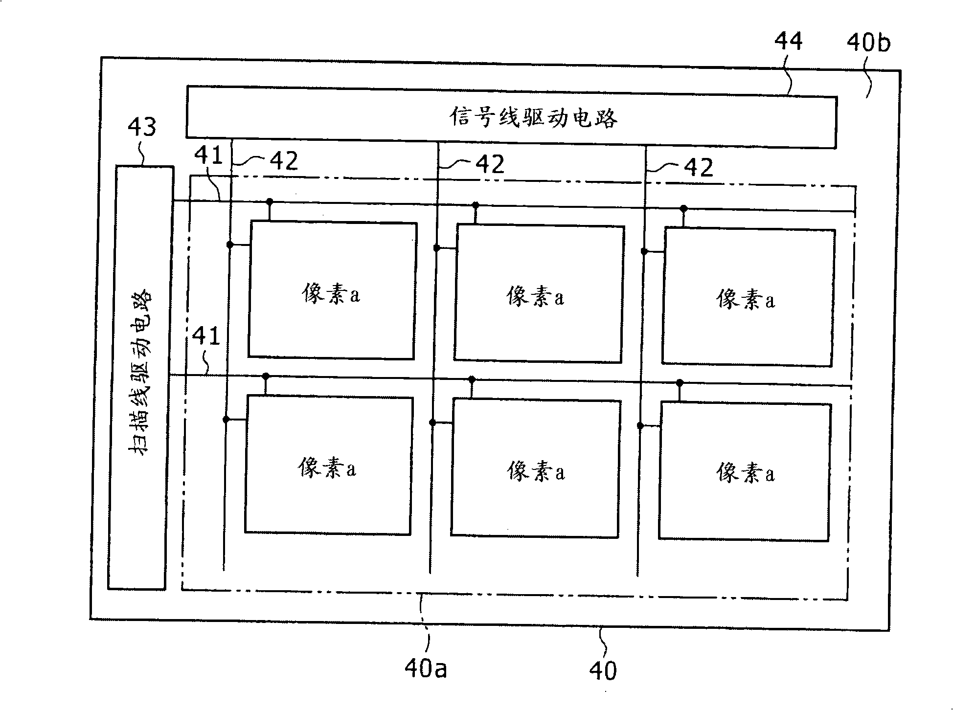
[0026] First, a display device will be described taking an organic EL display operable to cause the organic EL elements to emit light using TFTs as driving elements as an example.

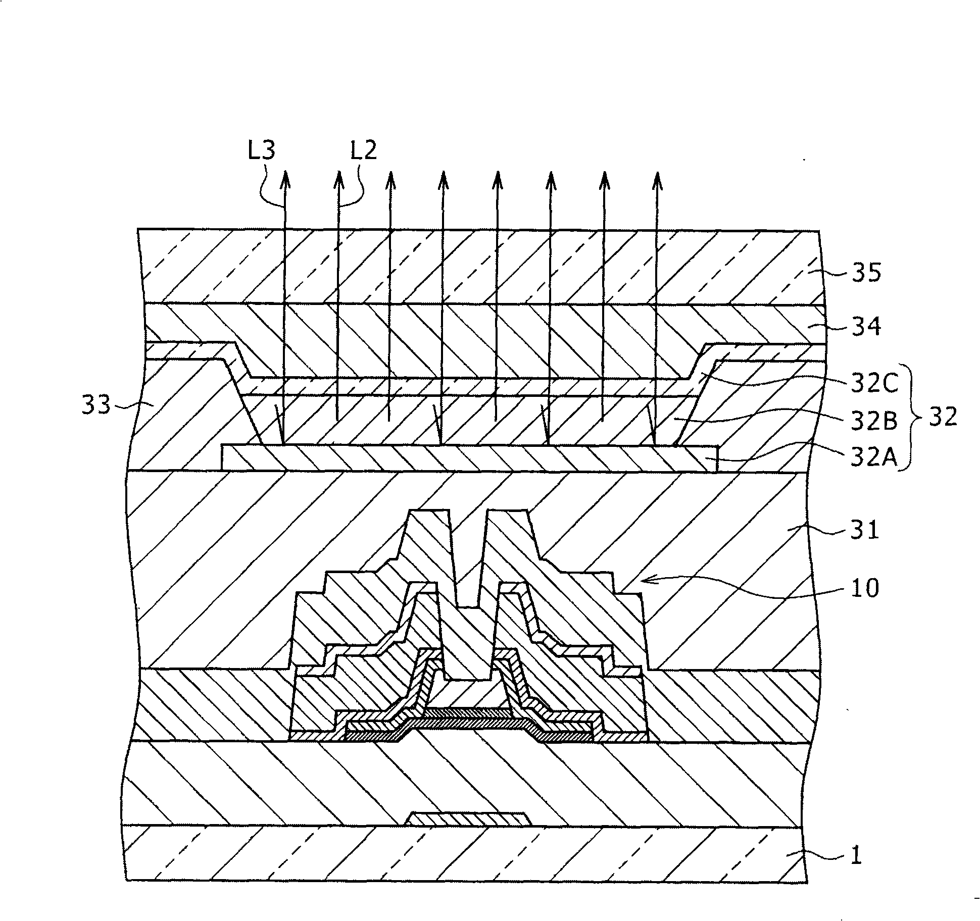
[0027] figure 1 is an explanatory diagram showing a configuration example of an organic EL display including TFTs.

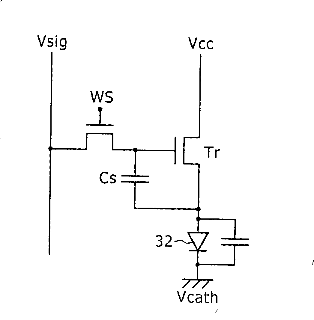
[0028] The organic EL display shown in the figure has a TFT 10 formed on an insulating substrate 1 as a driving element. In addition, the insulating planarization film 31 is uniformly formed on the TFT 10 . Furthermore, a plurality of organic EL elements 32 are formed. Each organic EL element 32 includes a reflective electrode 32A, an organic light emitting layer 32B, and a transparent electrode 32C. Furthermore, an inter-electrode insulating film 33 i...


PUM


Abstract

The present invention provides a film transistor, a manufacturing method thereof and a display using the film transistor. The film transistor manufacturing method includes the steps of: forming a gate electrode, gate insulating film and amorphous silicon film in succession on an insulating substrate; forming a channel protective film only in the region which will serve as a channel region of the amorphous silicon film; and forming an n-plus silicon film and metal layer on top of the channel protective film and amorphous silicon film in succession.; The method further includes the step of patterning the amorphous silicon film and n-plus silicon film to selectively leave the region associated with source and drain electrodes, using the channel protective film as an etching stopper to selectively remove the region of the n-plus silicon film and metal layer associated with the channel region so as to form source and drain regions from the n-plus silicon film and also form source and drain electrodes from the metal layer.

Description

technical field [0001] The present invention relates to a manufacturing method of a thin film transistor, a thin film transistor and a display using the thin film transistor. Background technique [0002] In recent years, a type of flat-panel display, that is, a display that uses organic EL (electroluminescence) to display images, has attracted much attention. Such a display or an organic EL display offers excellent characteristics including a wide viewing angle and low power consumption due to the light emission of the organic light emitting element itself. In addition, organic EL displays provide quick response to high-speed high-definition video signals. Therefore, efforts are being made to commercialize it, especially in imaging and other fields. [0003] Active matrix, a driving method of organic EL displays in which thin film transistors (TFTs) are used as driving elements, is superior to conventional passive matrices in response time and resolution. Therefore, this...

Claims


Application Information

Patent Timeline
Patent Type & Authority Applications(China)
IPC IPC(8): H01L21/336H01L29/786H01L27/32
Inventor 丰田基博荒井俊明
Owner SONY CORP
Why Eureka
Try Eureka