Field effect transistor, method for manufacturing the same and electronic device using the field effect transistor

A technology for field effect transistors and electronic equipment, applied in transistors, semiconductor/solid-state device manufacturing, nanotechnology for information processing, etc., can solve problems such as large deviations in threshold voltage characteristics, large deviations, and insufficient electrical contact with nanowires , to achieve the effect of small characteristic deviation, light weight and easy manufacture

Inactive Publication Date: 2007-04-18
PANASONIC CORP
View PDF2 Cites 0 Cited by
  • Summary
  • Abstract
  • Description
  • Claims
  • Application Information

AI Technical Summary

Problems solved by technology

[0004] However, in the method described in the above documents, the electrical contact between the nanowires and the electrodes, and the electrical contact between the nanowires are insufficient, and their deviations are also large.
Therefore, the FET obtained by the above-mentioned conventional method has a problem of large variation in characteristics such as threshold voltage.

Method used


Image

  • Field effect transistor, method for manufacturing the same and electronic device using the field effect transistor
  • Field effect transistor, method for manufacturing the same and electronic device using the field effect transistor
  • Field effect transistor, method for manufacturing the same and electronic device using the field effect transistor

Examples


Embodiment approach 1

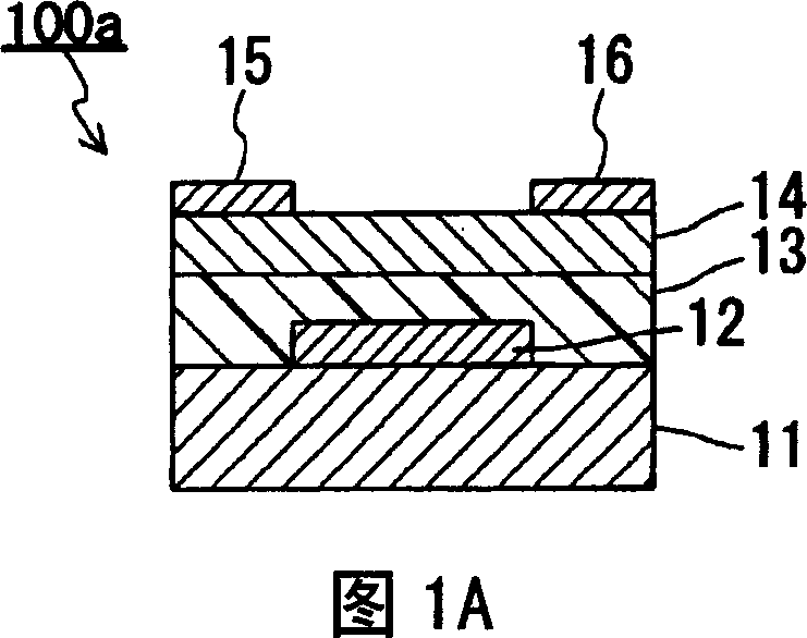
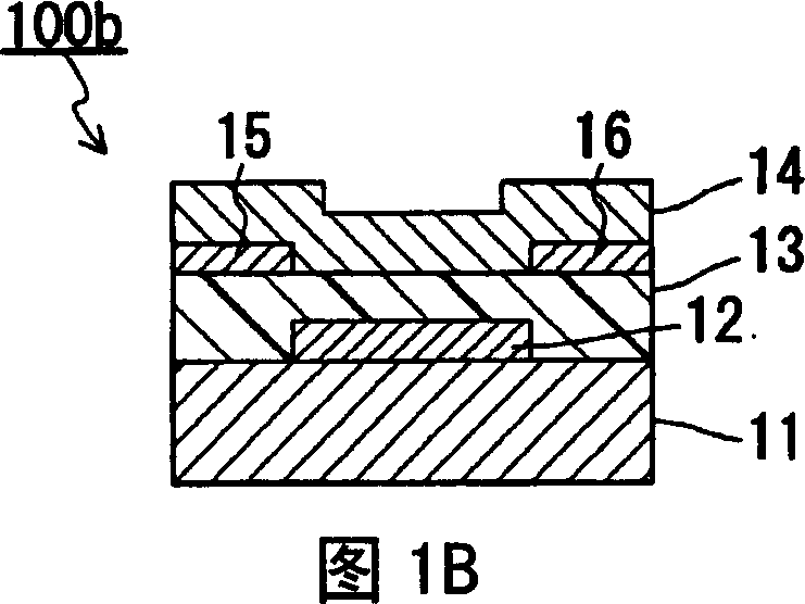
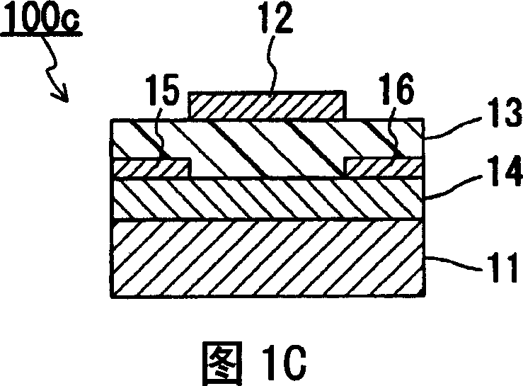
[0036] Next, examples of the FET of the present invention will be described. 1A to 1D are cross-sectional views schematically showing representative examples of the FET of the present invention. As shown in FIGS. 1A to 1D , there are various structures of the FET of the present invention. FETs 100 a to 100 d in FIGS. 1A to 1D include a substrate 11 , a gate electrode 12 , a gate insulating layer 13 , a semiconductor layer 14 , a source electrode 15 , and a drain electrode 16 . Part of the semiconductor layer 14 functions as a channel region. The source electrode 15 and the drain electrode 16 are usually in direct contact with the semiconductor layer 14 , but a layer for reducing connection resistance or the like may be disposed at the boundary between the two.

[0037]The gate electrode 12 usually faces the semiconductor layer 14 via the gate insulating layer 13 . The gate electrode 12 is an electrode that applies an electric field to at least the channel region, that is, t...

Embodiment approach 2

[0086] In Embodiment 2, an active matrix display, a wireless ID tag, and a portable device will be described by taking an electronic device including the FET of the present invention described in Embodiment 1 as an example.

[0087] As an example of an active matrix display, a display using organic EL as a display portion will be described. Fig. 6 is a partially exploded perspective view schematically showing the structure of the display.

[0088] The display shown in FIG. 6 includes drive circuits 150 arranged in an array on a plastic substrate 151 . The driving circuit 150 includes the FET of the present invention and is connected to the pixel electrode. An organic EL layer 152 , a transparent electrode 153 , and a protective film 154 are arranged on the drive circuit 150 . The organic EL layer 152 has a structure in which a plurality of layers such as an electron transport layer, a light emitting layer, and a hole transport layer are stacked. The source electrode line 15...


PUM


Abstract

A field effect transistor is provided with a semiconductor layer (14); a source electrode (15) and a drain electrode (16) which are electrically connected with the semiconductor layer (14); and a gate electrode (12) for applying electric field to the semiconductor layer (14) between the source electrode (15) and the drain electrode (16). The semiconductor layer (14) includes a plurality of fine wires, which are composed of inorganic semiconductor, and an organic semiconductor material.

Description

technical field [0001] The present invention relates to a field effect transistor, a manufacturing method thereof, and an electronic device using the field effect transistor. Background technique [0002] Field effect transistors (hereinafter sometimes referred to as "FETs") are used in various electronic devices such as active matrix displays. By using a plastic substrate in such an electronic device, a lightweight and flexible device can be obtained. However, in order to use a plastic substrate, it is necessary to form a semiconductor layer at a low temperature. [0003] As a method of forming a semiconductor layer of an FET at a low temperature, a method of forming a semiconductor layer using a semiconductor nanowire has been proposed. This method is described in, for example: Duan Xiangfeng (xiangfeng duan), etc., High-Performance thin-film transistors using semiconductor nanowires and nanoribbons (High-Performance thin-film transistors using semiconductor nanowires an...

Claims


Application Information

Patent Timeline
Patent Type & Authority Applications(China)
IPC IPC(8): H01L29/786H01L51/05H01L21/336
CPCB82Y10/00H01L51/0545H01L29/66742H01L51/0541H01L29/0665H01L29/78696H01L29/0673H10K10/464H10K10/466
Inventor 竹内孝之川岛孝启斋藤彻奥泽智宏北冈康夫
Owner PANASONIC CORP
Why Eureka
Try Eureka