
Insulated gate semiconductor device

An insulated gate, semiconductor technology, used in semiconductor devices, electrical components, circuits, etc., can solve problems such as on-resistance deviation, threshold voltage deviation, forward voltage deviation, etc., to reduce characteristic deviation, reduce on-resistance, The effect of expanding the chip size

Active Publication Date: 2012-10-17
SEMICON COMPONENTS IND LLC
View PDF5 Cites 0 Cited by
  • Summary
  • Abstract
  • Description
  • Claims
  • Application Information

AI Technical Summary

Problems solved by technology

[0008] However, it is known that in the strip-shaped trench gate structure as described above, voids are generated in the polysilicon filled in the trenches, and the voids cause characteristic deviations (on-resistance deviations, threshold voltage (Vp) deviations, forward voltage ( Cause of Vf) Deviation)

Method used


Image

  • Insulated gate semiconductor device
  • Insulated gate semiconductor device
  • Insulated gate semiconductor device

Examples


Embodiment Construction

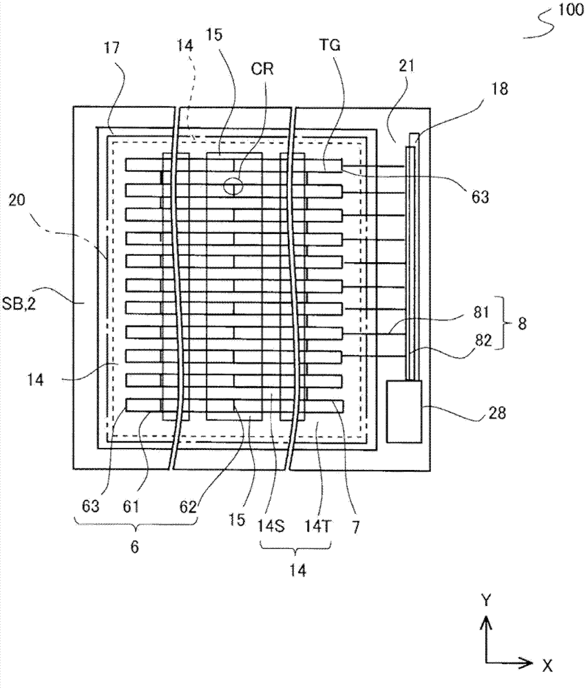
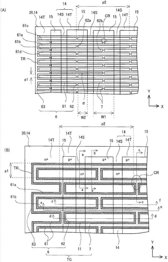
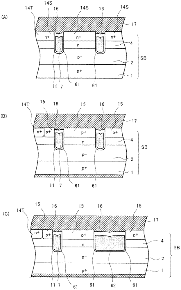
[0032] Taking the p-channel MOSFET as an example, refer to Figure 1 to Figure 4 Embodiments of the present invention will be described.

[0033] figure 1 It is a plan view of MOSFET 100 of this embodiment.

[0034] The substrate SB constituting the MOSFET 100 chip is formed by laminating a p − -type semiconductor layer 2 on a p + -type silicon semiconductor substrate (not shown). The p − -type semiconductor layer 2 is, for example, a silicon semiconductor layer formed on a p + -type silicon semiconductor substrate by, for example, epitaxial growth. The element region 20 (one-dot chain line) is provided on the surface of the p-type semiconductor layer 2 .

[0035] The element region 20 is covered with a source electrode 17 connected to a source region (not shown) of the MOSFET 100 .

[0036] The groove 6 has a first groove 61 , a second groove 62 and a third groove 63 . A plurality of first grooves 61 are provided parallel to each other in a strip shape extending along th...


PUM


Abstract

The invention discloses an insulated gate semiconductor device, the leading part of a gate lead wire leading the gate electrode of an MOSFET out of the surrounding of a substrate is not configured as an MOSFET having the same effect in an element region; namely if the gate lead wire is arranged along the periphery of a chip, the non-work region is increased, so that the situation of expanding the area of the element region and reducing the chip area are restrained. In the insulated gate semiconductor device, a gate lead wiring and an electrical conductor connecting the gate lead wiring to a protective diode are arranged in a straight line without bending along one and the same side of the chip. One bent portion or no bent portion is overlapped and extended on the upper parts of the gate lead wiring and the electrical conductor and connects them to the protective diode. Further, the protective diode is arranged adjacent to the electrical conductor or the gate lead wiring, and a portion of the protective diode is arranged in close proximity to a gate pad portion.

Description

technical field [0001] The present invention relates to an insulated gate type semiconductor device, in particular to an insulated gate type semiconductor device which contributes to lower on-resistance. Background technique [0002] In an insulated gate semiconductor device having a groove structure, a structure in which groove patterns are lattice-like in a planar view is known (for example, refer to Patent Document 1). [0003] In an insulated gate type semiconductor device having a trench structure, reduction of on-resistance is an important issue, and miniaturization of transistor cells (transistor cells) is being pursued as one of methods for solving this issue. As an example of miniaturization of transistor cells, there is known a structure in which an interlayer insulating film is buried in a trench to insulate a gate electrode buried in the trench from a source electrode provided on a substrate surface, and the substrate surface is flattened. In this structure, the...

Claims


Application Information

Patent Timeline
Patent Type & Authority Applications(China)
IPC IPC(8): H01L29/78H01L29/06H01L29/423
CPCH01L29/7397H01L29/4238H01L29/4236
Inventor 宫田拓司竹中一将
Owner SEMICON COMPONENTS IND LLC
Learn More