Stereo encapsulation structure
A technology of three-dimensional packaging and packaging, which is applied in the direction of electric solid-state devices, semiconductor devices, semiconductor/solid-state device components, etc., to achieve the effects of reducing electromagnetic interference, high line density, blocking or electromagnetic interference
- Summary
- Abstract
- Description
- Claims
- Application Information
AI Technical Summary
Problems solved by technology
Method used
Image

Examples
Embodiment Construction
[0054] The detailed description of some embodiments of the present invention is as follows. However, in addition to the detailed description, the present invention can also be widely implemented in other embodiments. That is, the scope of the present invention is not limited by the proposed embodiments, but should be subject to the scope of the patent application filed by the present invention. In addition, in order to provide a clearer description and make it easier to understand the present invention, the various parts in the drawings are not drawn according to their relative dimensions. Some dimensions have been exaggerated compared with other related dimensions; the irrelevant details are not completely drawn. , In order to simplify the drawings.
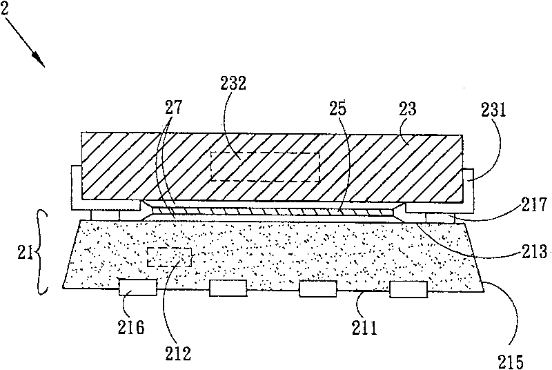
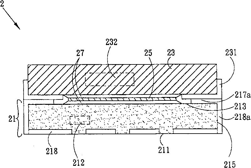
[0055] Such as figure 2 As shown, the three-dimensional package structure 2 of an embodiment of the present invention includes a semiconductor package 21, an energy storage element 23, and a shielding layer 25. The semiconductor ...
PUM
 Abstract
Description
Claims
Application Information