Flip-chip integrated encapsulation structure of LED and method thereof

A light-emitting diode and integrated packaging technology, which is applied in semiconductor/solid-state device manufacturing, electrical components, electric solid-state devices, etc., to achieve the effects of improving connection reliability, realizing automation and mass production, and solving heat dissipation problems

Inactive Publication Date: 2009-10-28
APT ELECTRONICS
View PDF0 Cites 43 Cited by
  • Summary
  • Abstract
  • Description
  • Claims
  • Application Information

AI Technical Summary

Problems solved by technology

It can be seen that the application of this packaging structure still requires gold wires, but the pad position of the gold wires is changed from the LED chip to the silicon substrate, but the shortcomings of the above-mentioned packaging structures have not been resolved.

Method used


Image

  • Flip-chip integrated encapsulation structure of LED and method thereof
  • Flip-chip integrated encapsulation structure of LED and method thereof
  • Flip-chip integrated encapsulation structure of LED and method thereof

Examples


Embodiment 1

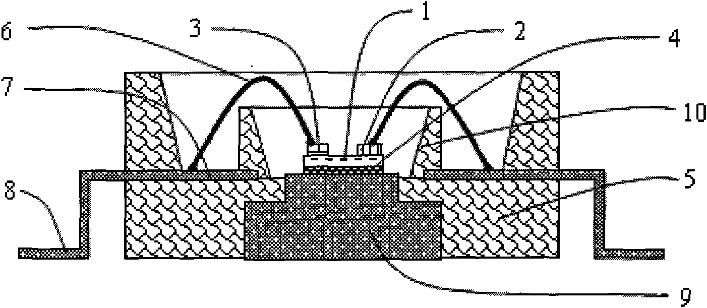
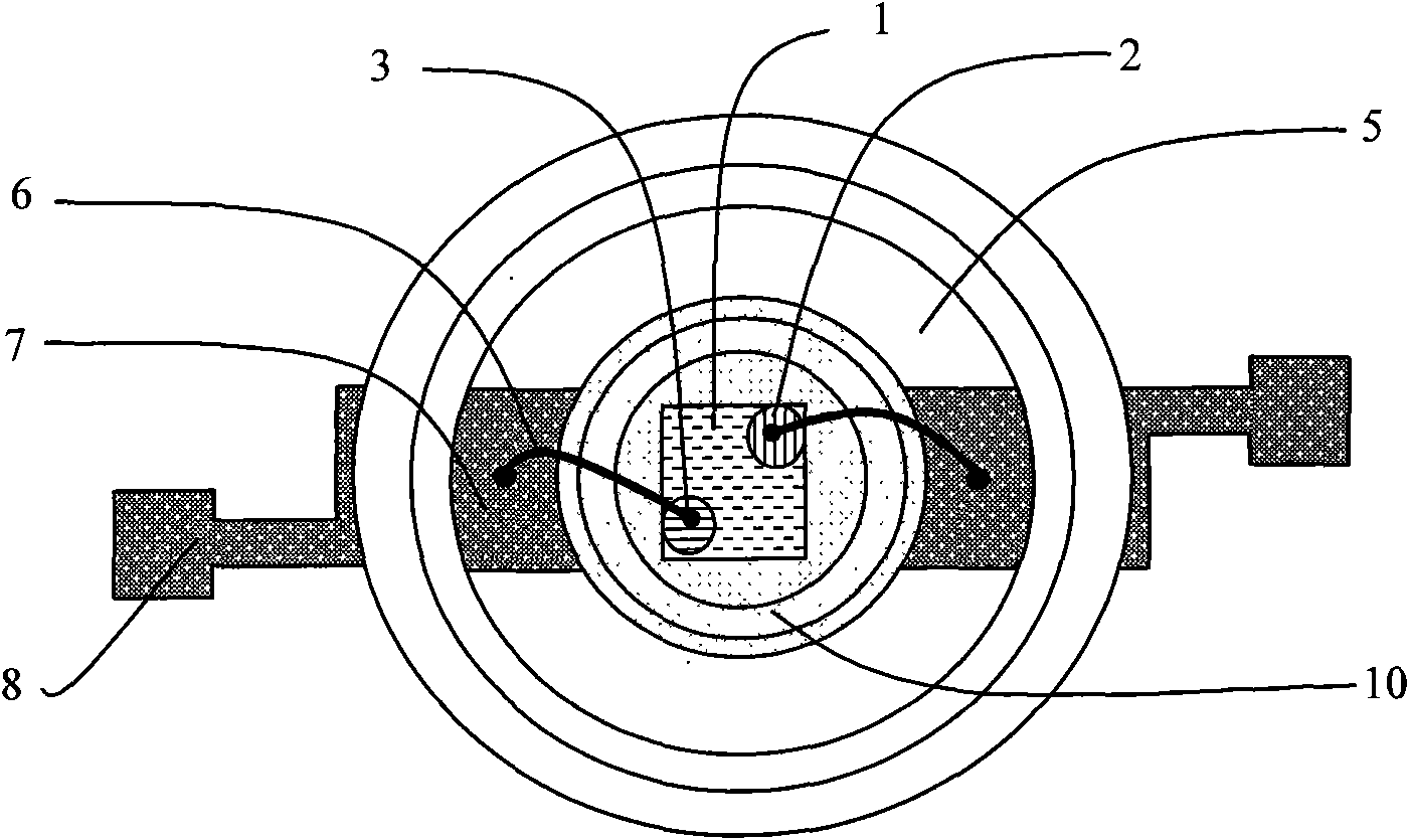
[0050] Such as Figure 2-1a and Figure 2-1b As shown, the light-emitting diode flip-chip integrated packaging structure uses the silicon wafer substrate 18 directly as the surface mount (SMD) support and heat dissipation channel for the entire structure of the LED chip 1 . A reflective cup is formed on the silicon wafer substrate 18, and the front side of the silicon wafer substrate 18 is provided with a front electrode connection layer 15, and at least one LED chip 1 is directly welded on the silicon wafer substrate with the reflective cup through metal bumps 14. 18 on the front electrode connection layer 15 to realize electrical connection. The front electrode connection layer 15 of the silicon substrate 18 is connected to the electrode metal pads 20 provided on the side and the back of the silicon substrate 18 through wiring on the side wall of the silicon groove. The front electrode connection layer 15 is electrically connected to the electrode metal pad 20 on the side ...

Embodiment 2

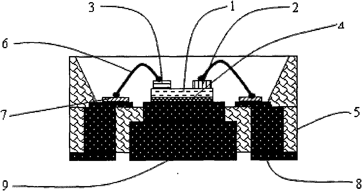
[0053] Such as Figure 2-2a and Figure 2-2b As shown, the light-emitting diode flip-chip integrated packaging structure uses the silicon wafer substrate 18 directly as the surface mount (SMD) bracket and heat dissipation channel supported by the entire structure of the LED chip 1, and a reflector cup is formed on the silicon wafer substrate 18. , the front surface of the silicon wafer substrate 18 is provided with a front electrode connection layer 15 . At least one LED chip 1 is directly flip-chip welded on the front electrode connection layer 15 of the silicon wafer substrate 18 with a reflective cup through the metal bump 14 to realize electrical connection. The front electrode connection layer 15 is connected to the electrode metal pad 20 provided on the back side of the silicon substrate 18 by means of through-hole wires in the silicon wafer substrate. The reflective cup can be formed by directly forming a silicon groove 21 on the silicon wafer substrate 18 as a reflec...

Embodiment 3

[0058] Such as Figure 3-1a , Figure 3-1b , Figure 3-1c , Figure 3-1d and Figure 3-1e As shown, here the connection between the front electrode connection layer 15 and the electrode metal pad 20 is mainly realized through the structure of the silicon groove side wall leads. The production steps are as follows:

[0059] (1) The LED chip 1 is manufactured. LED chip 1 is an epitaxial wafer grown on a sapphire substrate with multiple layers of gallium nitride. After a series of process steps such as photolithography, etching, metal layer deposition and passivation layer protection, the P electrode 2 and The N electrode 3 is fabricated.

[0060] (2) Fabricate a silicon wafer substrate 18 and form a reflective cup on the silicon wafer substrate 18 . The manufacturing steps are as follows: a, firstly fabricate the silicon wafer substrate 18 and the reflective cup wafer 16; b, then align the reflective cup wafer with the same characteristic size with the silicon wafer subst...


PUM


Abstract

The invention provides a novel light emitting diode (LED) encapsulation structure which directly adopts a silicon dice substrate as both a surface mounting bracket and a radiation channel of an integrated structure support of an LED chip; a front electrode connecting layer is arranged on the front surface of the silicon dice substrate; the front electrode connecting layer on the front surface of the silicon dice substrate is connected with an electrode metal bonding pad at the back of the silicon dice substrate through a lead of a silicon groove side-wall or a lead of a through-hole of the silicon dice substrate; and at least one LED chip is welded directly by flip-chip on the front electrode connecting layer of the silicon dice substrate with an optical source through a metal bump. The invention also provides a method for manufacturing the LED encapsulation structure. The invention avoids steps of die bonding and gold-wire welding and enhances the connection reliability of chips and especially the connection reliability of multi-chip modules; and the invention leads the encapsulation of high-power LED and especially the encapsulation of multi-chip module to be miniaturized and also leads power-supply drive and circuits of LED protection and the like to be integrated on the silicon dice so as to provide a systematic and integrated encapsulation proposal for high-power LED illumination.

Description

technical field [0001] The invention relates to the field of manufacturing and assembling of light-emitting diodes, specifically based on silicon processing technology, a light-emitting diode flip-chip welding integrated packaging structure and its production are directly flipped into a silicon integrated packaging structure with reflective cups. method. Background technique [0002] The structure of gallium nitride-based (GaN) light-emitting diodes (LEDs) is mostly first grown on a sapphire substrate by epitaxially growing multiple layers of gallium nitride (GaN) crystal layers, and then through the manufacturing process on the P of the LED chip. Metal electrodes are respectively drawn out from the N-type area and the N-type area, as shown in Figures 1-1 and 1-2, metal electrodes--P electrodes 2 and N electrodes 3 are formed on the chip 1. The usual assembly method of traditional LEDs is to mount and fix the LED chip 1 in the packaging bracket 5 with the thermal interface ...

Claims


Application Information

Patent Timeline
Patent Type & Authority Applications(China)
IPC IPC(8): H01L33/00H01L25/075H01L21/48H01L21/50
CPCH01L2924/10253H01L2224/45144H01L2224/48091H01L2224/73265H01L2224/48247
Inventor 肖国伟曾照明周玉刚侯宇
Owner APT ELECTRONICS
Why Eureka
Try Eureka