Semiconductor device and method for manufacturing the same

A technology of semiconductors and devices, which is applied in the field of semiconductor devices and their manufacturing, and can solve problems such as unbalanced correction of device characteristics

Inactive Publication Date: 2009-01-14
INFINEON TECH AG
View PDF0 Cites 14 Cited by
  • Summary
  • Abstract
  • Description
  • Claims
  • Application Information

AI Technical Summary

Problems solved by technology

This will lead to an unbalanced correction of negative channel M

Method used


Image

  • Semiconductor device and method for manufacturing the same
  • Semiconductor device and method for manufacturing the same
  • Semiconductor device and method for manufacturing the same

Examples


Embodiment Construction

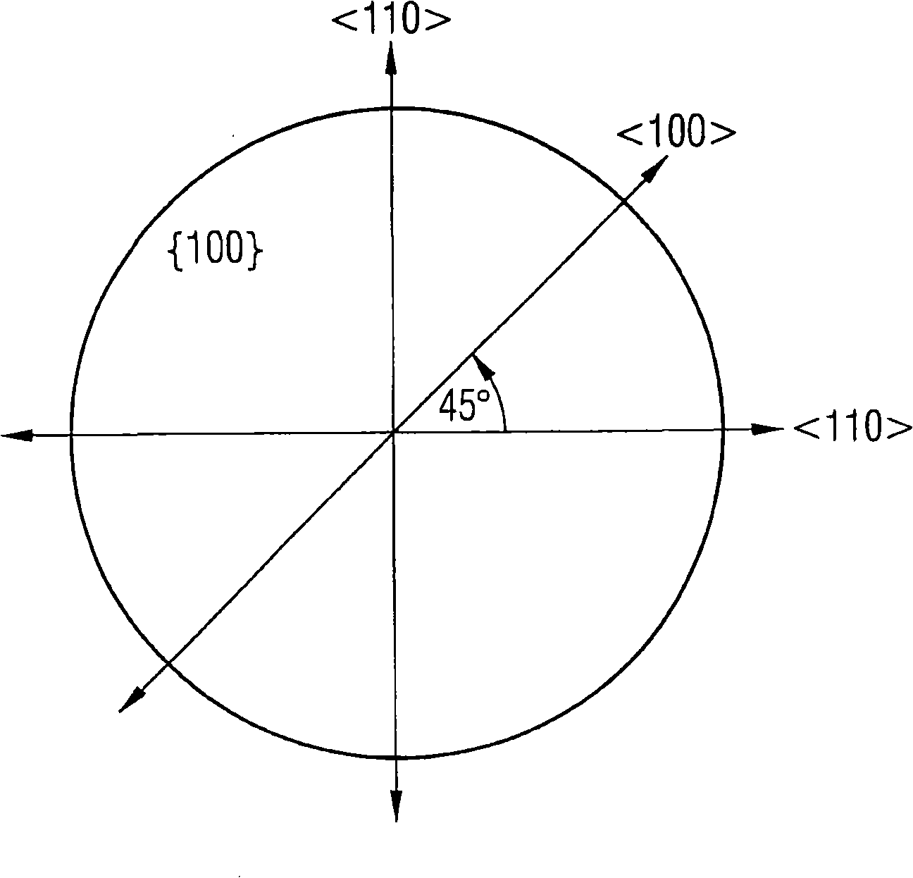
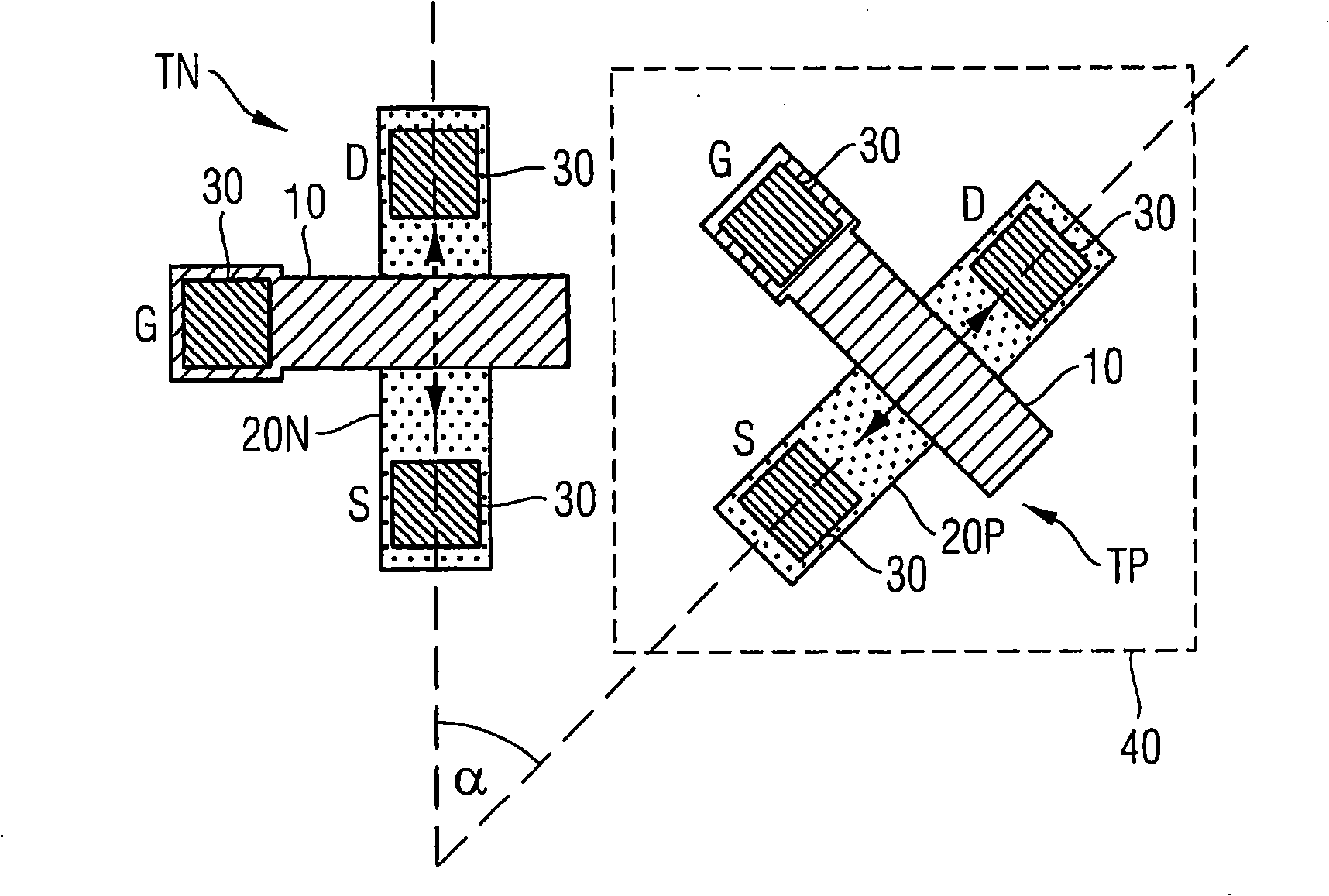
[0014] The various aspects outlined above can be implemented in a variety of ways. The following description illustrates various examples of implementing these aspects. It should be understood that other examples can also be used, and the structure and function can be modified without departing from the scope of the present invention.

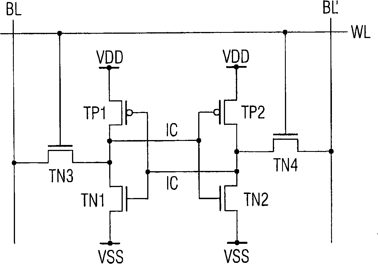
[0015] Unless expressly stated otherwise, two or more elements referred to herein are "coupled" or "connected" to each other and are meant to include in a broad sense, (a) without intervening elements, elements directly connected to each other, or directly communicating with each other, and (b) Through one or more intermediate elements, the elements are indirectly connected to each other or indirectly communicate with each other. Moreover, it should be realized that the functional blocks or units shown in the figures may be implemented with separate circuits in some embodiments, but may also be implemented in whole or in part by common circuits in ...


PUM


Abstract

A semiconductor device and method of manufacturing thereof. The semiconductor device has at least one NMOS device and at least one PMOS device provided on a substrate. An electron channel of the NMOS device is aligned with a first direction. A hole channel of the PMOS device is aligned with a different second direction that forms an acute angle with respect to the first direction.

Description

Technical field [0001] The present invention relates to a semiconductor device and a manufacturing method thereof. Background technique [0002] According to planar complementary metal oxide semiconductor (complementary MOS, or CMOS) technology, complementary carrier type field effect transistors are formed on a semiconductor substrate, such as a bulk silicon substrate with {100}-type surface orientation. In the manufacturing process of such a semiconductor device, an electron channel or a hole channel is formed by patterning a functional layer formed on a semiconductor substrate. The functional layer is, for example, a doped semiconductor material layer, a metal layer, or an oxide layer. The patterned structure is usually aligned with a specific crystal orientation of the semiconductor substrate, and the specific crystal orientation is indicated by a plane or notch around the semiconductor wafer. [0003] As the lateral feature size of the semiconductor structure decreases, espe...

Claims


Application Information

Patent Timeline
IPC IPC(8): H01L21/8238H01L27/092
CPCH01L27/1104H01L27/0207H01L21/823807H10B10/12
Inventor A·休伯W·坎普M·奥斯特迈尔
Owner INFINEON TECH AG
Why Eureka
Try Eureka