Image pickup apparatus, image processing method, and computer program

An image pickup device and image processing technology, which is applied in image communication, radiation control devices, televisions, etc., can solve the problems of not realizing correction processing of large image pickup devices, etc.

Inactive Publication Date: 2009-01-21
SONY CORP
View PDF3 Cites 21 Cited by
  • Summary
  • Abstract
  • Description
  • Claims
  • Application Information

AI Technical Summary

Problems solved by technology

[0009] However, image correction processing by dark current cancellation developed earlier is basically a processing compatible with small image pickup devices manufactured by a single exposure process, and correction processing compatible with large image pickup devices has not been realized, which Large image pickup devices have device areas with different characteristics caused by the above-mentioned multiple manufacturing processes

Method used


Image

  • Image pickup apparatus, image processing method, and computer program
  • Image pickup apparatus, image processing method, and computer program
  • Image pickup apparatus, image processing method, and computer program

Examples


no. 1 example

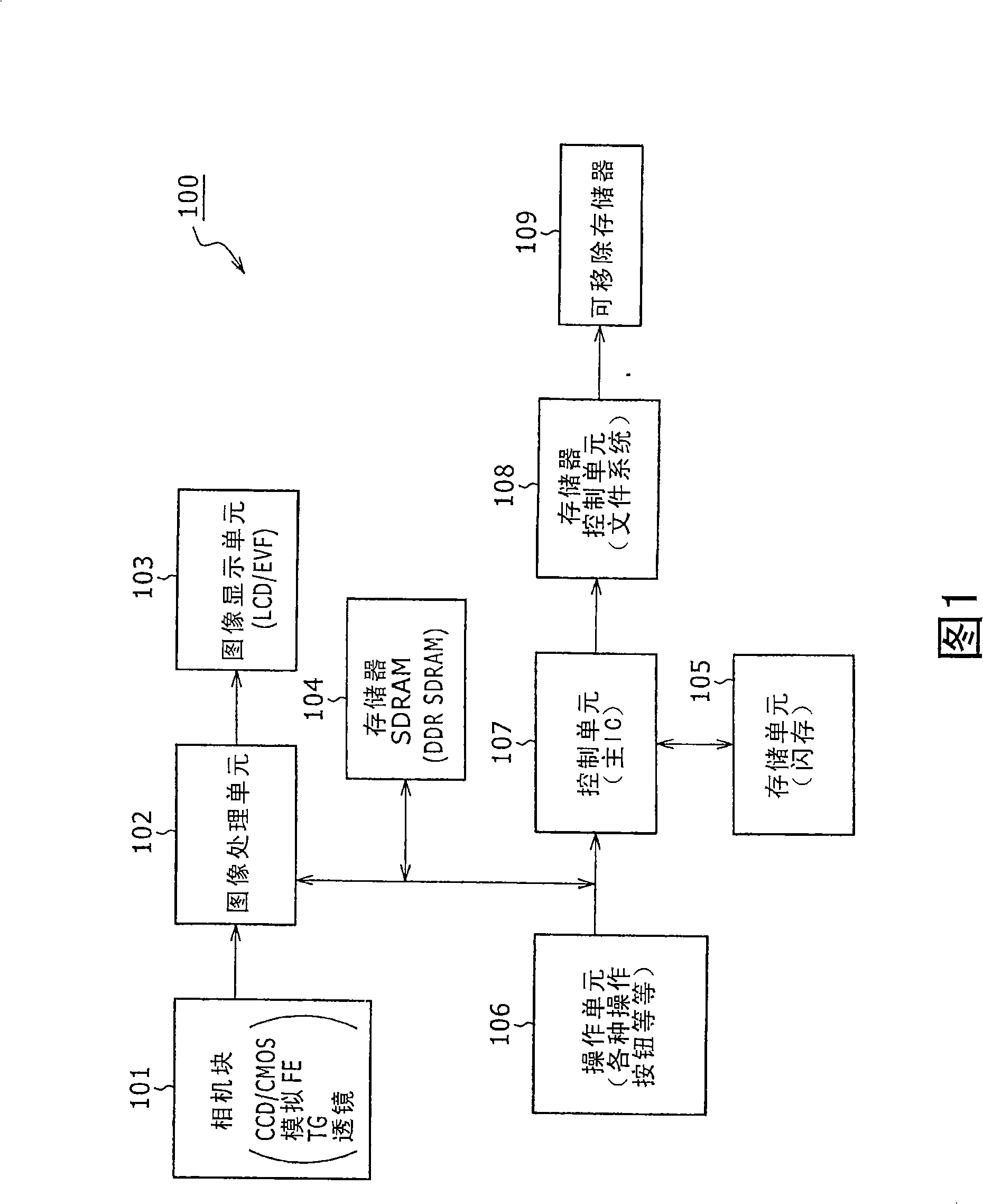
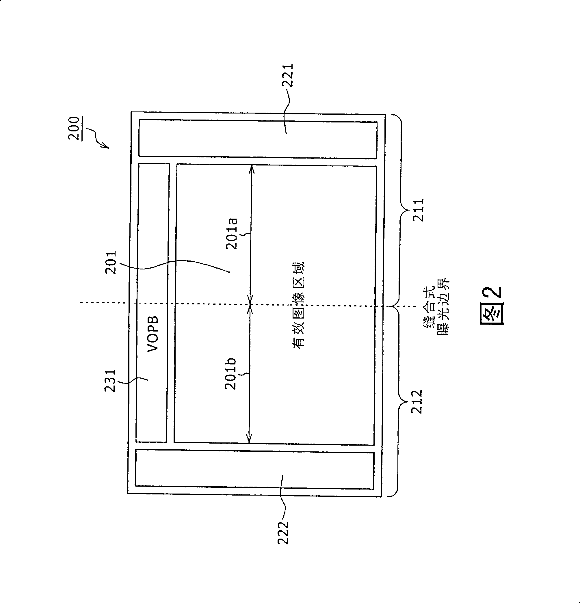
[0072] FIG. 2 shows a configuration example of an image pickup device 200 used in the image pickup apparatus according to the embodiment of the present invention. The image pickup device 200 is manufactured by stitch exposure in which formation of a circuit is performed through a plurality of exposure processes in a manufacturing stage. Therefore, the image pickup device has a plurality of imaging planes (divided areas) with different characteristics. The image pickup device 200 shown in FIG. 2 is a CMOS divided into two by stitch exposure. In the following, the right plane of the image pickup device 200 is referred to as a first imaging plane 211 , and the left plane is referred to as a second imaging plane 212 . Each imaging surface 211, 212 corresponds to a unit area of ​​an exposure process in a manufacturing stage, and has different characteristics.

[0073] The image pickup device 200 has an effective image area 201 for receiving incident light during shooting, and an ...

no. 2 example

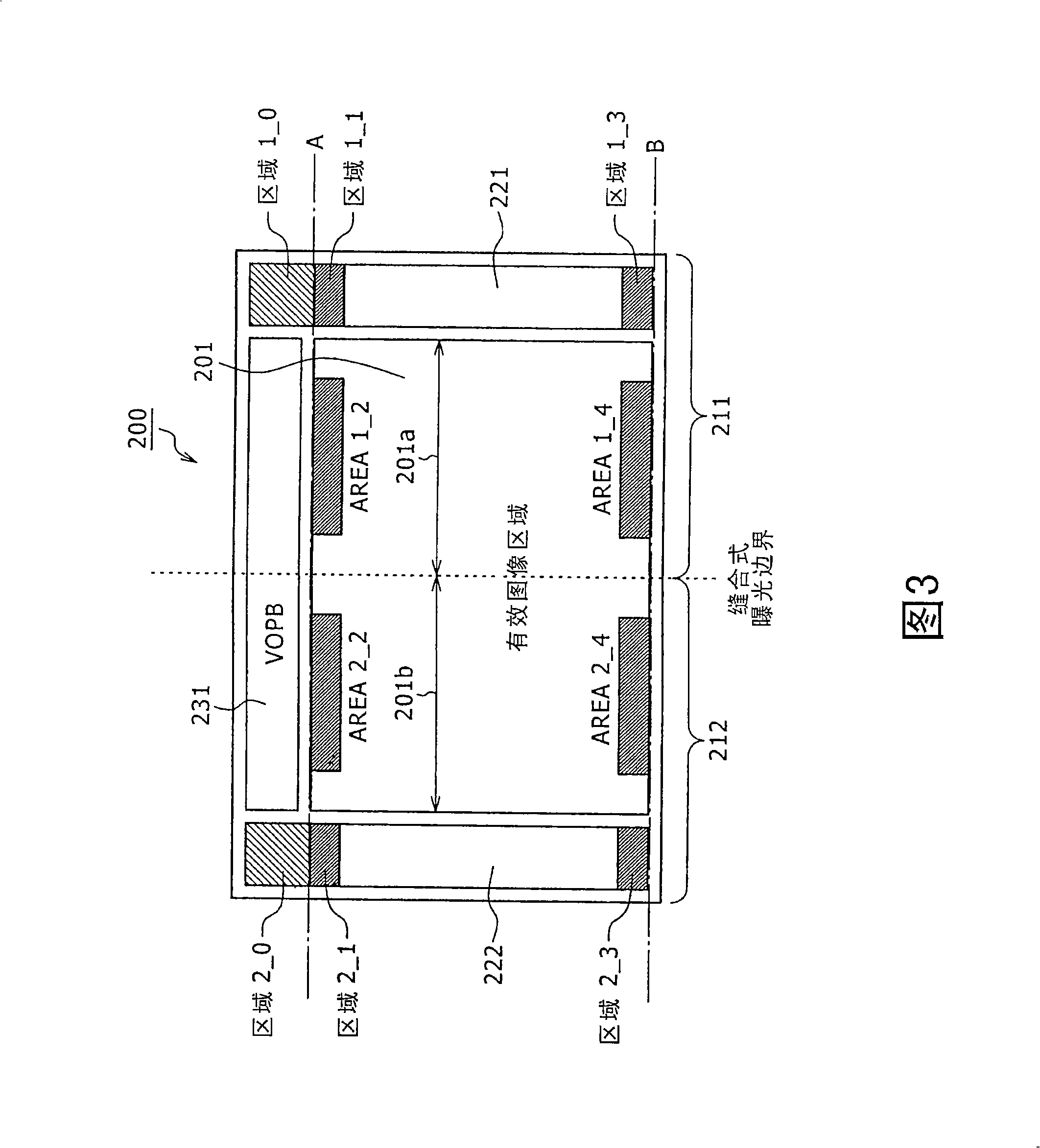
[0229] The first embodiment described above requires a structure in which individual HOPB areas are provided corresponding to each imaging plane having different characteristics, and the HOPB area is provided corresponding to each imaging plane. However, when producing an actual image pickup device, it is required to set a small HOPB area in order to set a large effective image area. For example, there is a structure in which one HOPB area is set for two imaging planes having different characteristics. Also, for example, if there are three or more imaging planes with different characteristics, setting one HOPB area for each imaging plane may not be preferable because the area of ​​the effective image area becomes small. In the second embodiment, the structure of an image pickup device in which the number of HOPB areas is smaller than the number of imaging planes having different characteristics (instead of setting the respective HOPB areas corresponding to imaging planes havin...


PUM


Abstract

The present invention discloses an image pickup apparatus and an imaging processing method. The image pickup apparatus includes an image pickup device including a plurality of imaging planes each having different dark current characteristics, and an image processing unit for receiving a signal from the image pickup device and performing an image generating process. The image processing unit calculates a dark current estimated to be generated in each of the plurality of imaging planes, independently for each imaging plane, and performs a dark current eliminating process on the basis of a dark current value calculated for each imaging plane.

Description

technical field [0001] The present invention relates to an image pickup device, an image processing method, and a computer program. More specifically, the present invention relates to an image pickup device, such as a digital camera, that performs a process of eliminating a dark current component of an image pickup device, an image processing method, and a computer program. Background technique [0002] An image pickup apparatus such as a digital camera has an image pickup device such as a complementary metal oxide semiconductor (CMOS) and a charge-coupled device (CCD), and is configured to convert an optical signal into an electric signal at the image pickup device processing to generate captured images. [0003] Image pickup devices equipped in many commonly used cameras are small image pickup devices smaller than 35 mm film (36×24 mm), for example. However, in recent years, cameras equipped with large image pickup devices having a greater number of effective pixels and ...

Claims


Application Information

Patent Timeline
Patent Type & Authority Applications(China)
IPC IPC(8): H04N5/217H01L27/146H04N5/335H04N5/361H04N5/369H04N5/372H04N5/374
CPCH04N5/3653H04N5/361H04N25/63H04N25/672H04N23/00H04N25/60
Inventor 来马大介佐藤伸行
Owner SONY CORP
Why Eureka
Try Eureka