Pixel construction and thin-film transistor thereof

A technology of thin-film transistors and semiconductors, which is applied in the direction of transistors, electric solid-state devices, semiconductor devices, etc., and can solve problems such as inconsistent feed-through voltages of thin-film transistors

Inactive Publication Date: 2009-02-04
AU OPTRONICS CORP
View PDF0 Cites 21 Cited by
  • Summary
  • Abstract
  • Description
  • Claims
  • Application Information

AI Technical Summary

Problems solved by technology

[0010] In view of this, the object of the present invention is to provide a pixel structure and its thin film tr...

Method used


Image

  • Pixel construction and thin-film transistor thereof
  • Pixel construction and thin-film transistor thereof
  • Pixel construction and thin-film transistor thereof

Examples


Embodiment Construction

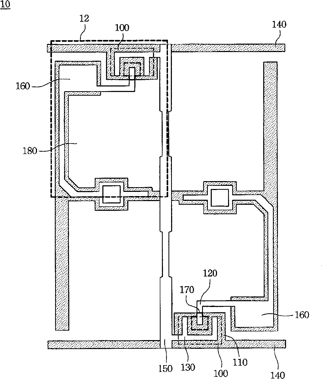
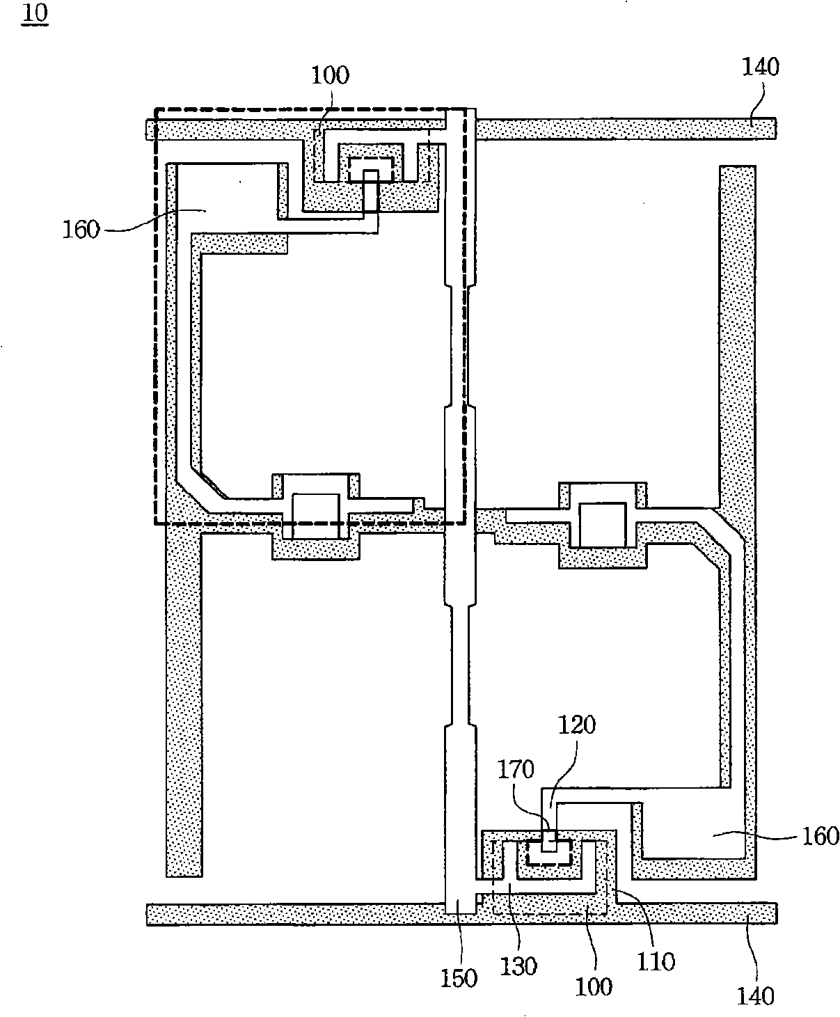
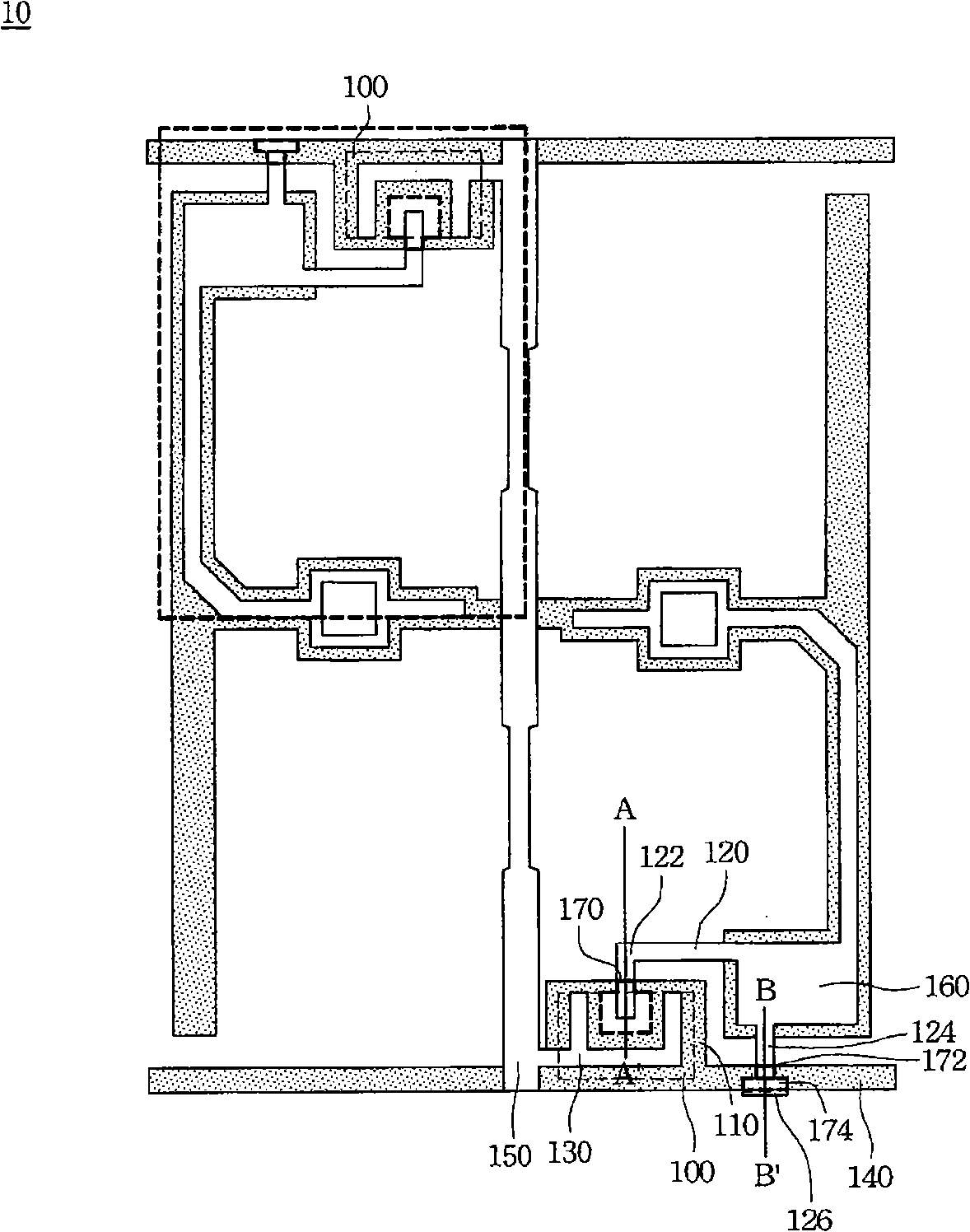
[0051] Please refer to Figure 2A , which shows a top view of the pixel structure 10 according to an embodiment of the present invention. The pixel structure 10 mainly has several thin film transistors 100 arranged in an array. Each TFT 100 has a gate 110 , a drain 120 and a source 130 , wherein the gate 110 is electrically connected to the scan line 140 , and the source 130 is electrically connected to the data line 150 .

[0052] Please also refer to Figure 2A to Figure 2C . Figure 2B show according to Figure 2A An enlarged cross-sectional view of the line AA' shown in , Figure 2C show according to Figure 2A An enlarged cross-sectional view of the BB' connection shown in .

[0053]Taking the bottom gate structure as an example, the gate 110 and the scan line 140 are both disposed on the substrate 200 . An insulating layer 210 is adjacent to cover the gate 110 and the scan line 140 . Next, a semiconductor layer 220 is covered on the insulating layer 210 . A drai...


PUM


Abstract

The invention discloses a pixel structure and a thin-film transistor. A grid connecting scanning line of the thin-film transistor is arranged at one surface of an insulating layer, and a semiconductor layer, a source electrode and a drain electrode are arranged at the other surface of the insulating layer. The source electrode is connected with a data line and the semiconductor layer. The first branch of the drain electrode is connected with the semiconductor layer and is partially aligned and superposed with the grid so as to induce parasitic capacitance. The second branch and the first branch of the drain electrode extend in the same direction and perpendicularly go across from above the scanning line. The second branch is partially aligned and superposed with the scanning line so as to induce a first compensation capacitance. A compensation electrode is connected with the second branch and is partially vertically arranged above the scanning line so as to induce a second compensation capacitance. The width of the line of compensation electrode is the total of the widths of the lines of first and second branches, so that the total of the parasitic capacitance, the first compensation capacitance and the second compensation capacitance is constant. The invention provides a pixel structure and a thin-film transistor and can solve the problem of uneven feed-through voltage due to displacement deviation of the two metal layers.

Description

technical field [0001] The present invention relates to a thin film transistor, and in particular to the layout of a thin film transistor array. Background technique [0002] In recent years, many flat panel display (Flat Panel Display) technologies have been developed successively, such as liquid crystal display (Liquid Crystal Display; LCD). Due to the advantages of thin, light and small, low power consumption, no risk of radiation, flat right-angle display, and stable and non-flickering images, liquid crystal displays will gradually become the mainstream of future displays. [0003] Thin Film Transistor-Liquid Crystal Display (TFT-LCD) is a type of flat-panel display. Its panel can be regarded as a layer of liquid crystal sandwiched between two glass substrates. The upper glass substrate is a color filter. Combination, the lower glass substrate has a thin film transistor array embedded on it. [0004] see Figure 1A , which is a schematic top view of a conventional thin...

Claims


Application Information

Patent Timeline
IPC IPC(8): H01L29/786H01L29/417H01L27/12H01L23/522G02F1/1362
Inventor 萧嘉强沈光仁陈培铭郑景升
Owner AU OPTRONICS CORP
Why Eureka
Try Eureka