Display device

A display device, display panel technology, applied in the direction of static indicators, optics, instruments, etc.

Active Publication Date: 2009-04-01
JAPAN DISPLAY INC +1
View PDF0 Cites 32 Cited by
  • Summary
  • Abstract
  • Description
  • Claims
  • Application Information

AI Technical Summary

Problems solved by technology

These problems are described below

Method used


Image

  • Display device
  • Display device
  • Display device

Examples


Embodiment 1

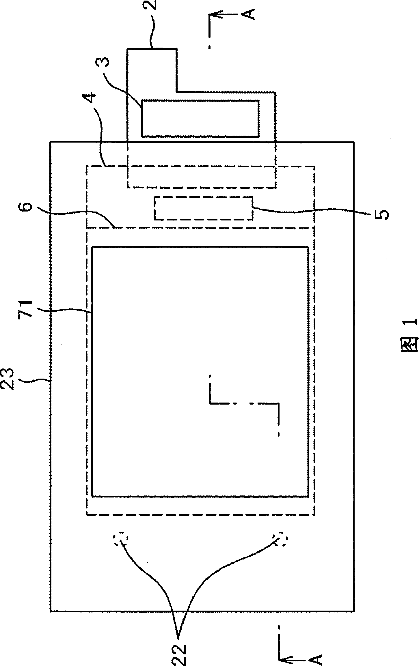
[0042] FIG. 1 is a plan view of a liquid crystal display device with a touch panel according to the present invention. In FIG. 1 , the touch panel 23 can be seen on the front surface. The touch panel 23 is covered with the light shielding layer 14 except for the display area 71 . Air holes 22 are formed in the film 11 with the lower transparent electrode on the back side of the touch panel 23 to allow outside air to flow through the inside of the touch panel 23 . The touch panel 23 is bonded to the color filter substrate 6 side of the liquid crystal display panel 24 .

[0043] In FIG. 1 , the TFT substrate 4 side is mounted with the drive IC 5 , the flexible wiring substrate 2 , and the like, so the TFT substrate 4 is larger than the color filter substrate 6 . The flexible wiring board 2 is connected to a liquid crystal display panel 24 and an external circuit, and various electronic components 3 are mounted thereon.

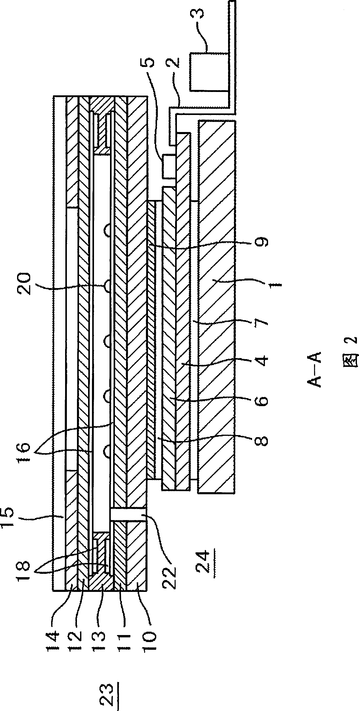
[0044] Fig. 2 is a cross-sectional view along line A-A ...

Embodiment 2

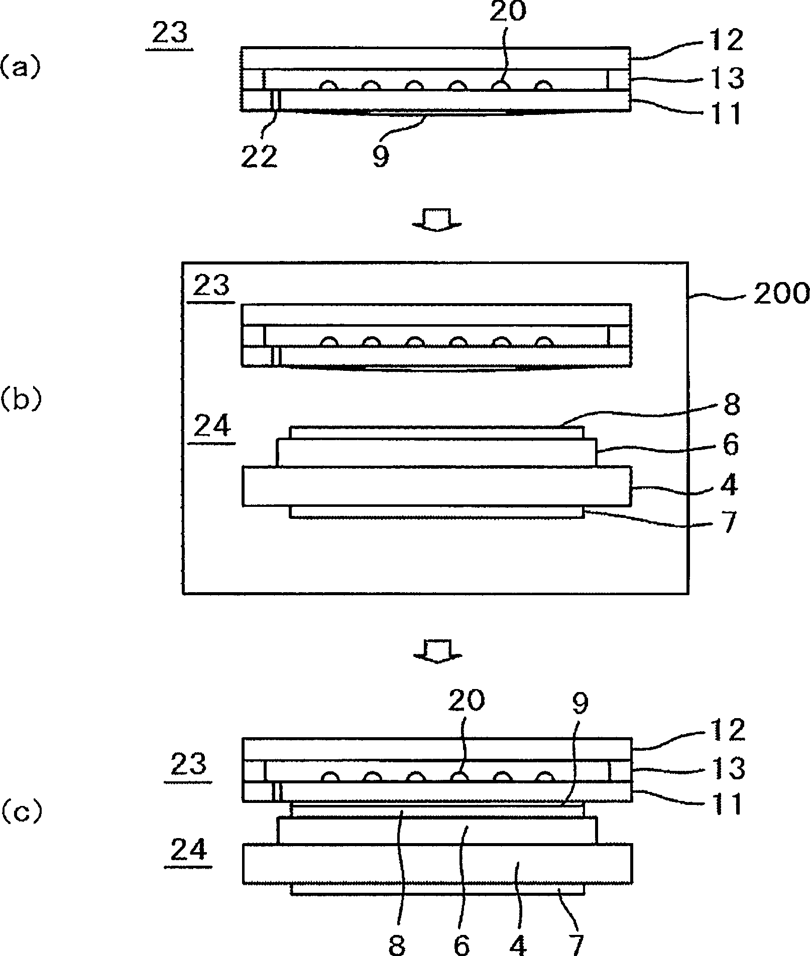
[0061] 6 is a cross-sectional view of a second embodiment of a liquid crystal display device with a touch panel according to the present invention. Most of the structure of FIG. 6 is the same as that of FIG. 2 explained in Embodiment 1. The difference from FIG. 2 is that the air holes 22 formed in the film 11 with the lower transparent electrode and the base substrate 10 are blocked. FIG. 6 shows an example in which the air hole 22 is blocked with an adhesive tape 25, but the present invention is not limited thereto, and may be blocked with resin or the like. As the resin, epoxy resin, silicone resin, or the like can be used.

[0062] In this way, by closing the air hole 22 , foreign matter can be prevented from entering the touch panel from the outside. In addition, it is possible to prevent intrusion of moisture, corrosive gas, and the like from the outside, and to prevent an increase in resistance of wiring 18 inside the touch panel, ITO 16 , and the like. In addition, b...

Embodiment 3

[0066] On the touch panel 23 , the film 12 with an upper transparent electrode and the film 11 with a lower transparent electrode face each other with a small gap therebetween. When the interval between the film 12 with the upper transparent electrode and the film 11 with the lower transparent electrode decreases, there is a case where a so-called Newton's ring occurs with respect to a specific wavelength. Newton rings degrade the image quality, so you need to prevent this from happening. By providing the air hole 22 in the touch panel 23, the air pressure inside the touch panel may decrease, and the film 12 with the transparent electrode may bend. In this way, the distance between the film 12 with the upper transparent electrode and the film 11 with the lower transparent electrode can be easily reduced. This bending can be reduced by closing the air hole 22 , but it is difficult to seal the air hole 22 .

[0067] The present embodiment provides a structure that suppresses t...


PUM


Abstract

In a display device having a touch panel, it is possible to prevent the generation of a screen defect caused by the intrusion of air bubbles into a UV curing resin formed between a touch panel and a display panel. The touch panel is constituted of an upper transparent-electrode-attached film 12 and a lower transparent-electrode-attached film 11, and an air hole 22 is formed in the lower transparent-electrode-attached film 11. Due to such constitution, in adhering the touch panel and the display panel to each other in a vacuum using a UV curing resin 9, air in the touch panel is also discharged and hence, there is no possibility that the touch panel swells. Accordingly, it is possible to prevent warping of the lower transparent-electrode-attached film 11 and hence, in curing the UV curing resin 9 for adhering the touch panel and the display panel to each other, it is possible to prevent the entanglement of air into the UV curing resin. Accordingly, a touch-panel attached display device free from a screen defect attributed to air bubbles can be manufactured.

Description

technical field [0001] The present invention relates to a display device, and more particularly, to a display device with a touch panel. Background technique [0002] Liquid crystal display devices are being used in various fields because they can be made small and thin. Examples are portable phones, PDAs, and the like. Among these devices, there is a method of using a touch panel as an input device. There are capacitive touch panels, resistive touch panels, etc., but resistive touch panels are widely used. The resistive touch panel is to make the transparent electrode formed on the film with the transparent electrode and the transparent electrode formed on the film with the lower transparent electrode transparent by pressing the film with the transparent electrode opposite to the film with the transparent electrode with the human finger or a stylus. The transparent electrodes on the film of electrodes are contacted, whereby the positional information is retrieved. [00...

Claims


Application Information

Patent Timeline
Patent Type & Authority Applications(China)
IPC IPC(8): G02F1/133G06F3/041
CPCG02F2202/28G02F2202/023G02F1/13338G06F3/0412
Inventor 三岛康之小林节郎樋口孝行
Owner JAPAN DISPLAY INC
Why Eureka
Try Eureka