Method and device for measuring modulation transfer function value

A modulation transfer function and measurement device technology, which is applied in the field of lens inspection, can solve problems such as low measurement efficiency, wrong measurement results, and increased measurement costs, and achieve the effect of improving measurement accuracy and detection efficiency

Inactive Publication Date: 2009-04-22
HONG FU JIN PRECISION IND (SHENZHEN) CO LTD +1
0 Cites 13 Cited by

AI-Extracted Technical Summary

Problems solved by technology

However, when the measuring device 100 is used, once the test board 10 has more patterns and the size of the test board 10 is larger than the sensing area of ​​the image sensor 40, the image sensor 40 cannot image all the patterns of the test board 10 at one time. The imaging luminance of the pattern sensed by the pixels of the image sensor...

Abstract

The invention relates to a device for measuring modulation transfer function values. The device comprises a testing plate, an image sensor, a bearing device and a drive device. The testing plate is provided with a plurality of alternate dark and bright patterns, the bearing device is arranged between the testing plate and the image sensor, and comprises a limit device and a bearing table, the limit device is arranged on the bearing table, and is opposite to the image sensor, and the bearing table is opposite to the testing plate. The drive device is used for driving the bearing device to move or rotate parallel to the testing plate so as to adjust the relative position between the bearing device and the testing plate, thus the image sensor is caused to respectively sense images of the patterns of different parts on the testing plate, and the images are formed by a lens to be tested. The invention further provides a method for measuring the modulation transfer function values. The device can help improve the measurement accuracy, and measure the modulation transfer function values of a plurality of lenses at a time, thus effectively improving the measurement efficiency.

Application Domain

Technology Topic

Image

  • Method and device for measuring modulation transfer function value
  • Method and device for measuring modulation transfer function value
  • Method and device for measuring modulation transfer function value

Examples

  • Experimental program(1)

Example Embodiment

[0018] The measuring device and measuring method of the modulation transfer function value of the technical scheme will be further described in detail below in conjunction with the accompanying drawings and embodiments.
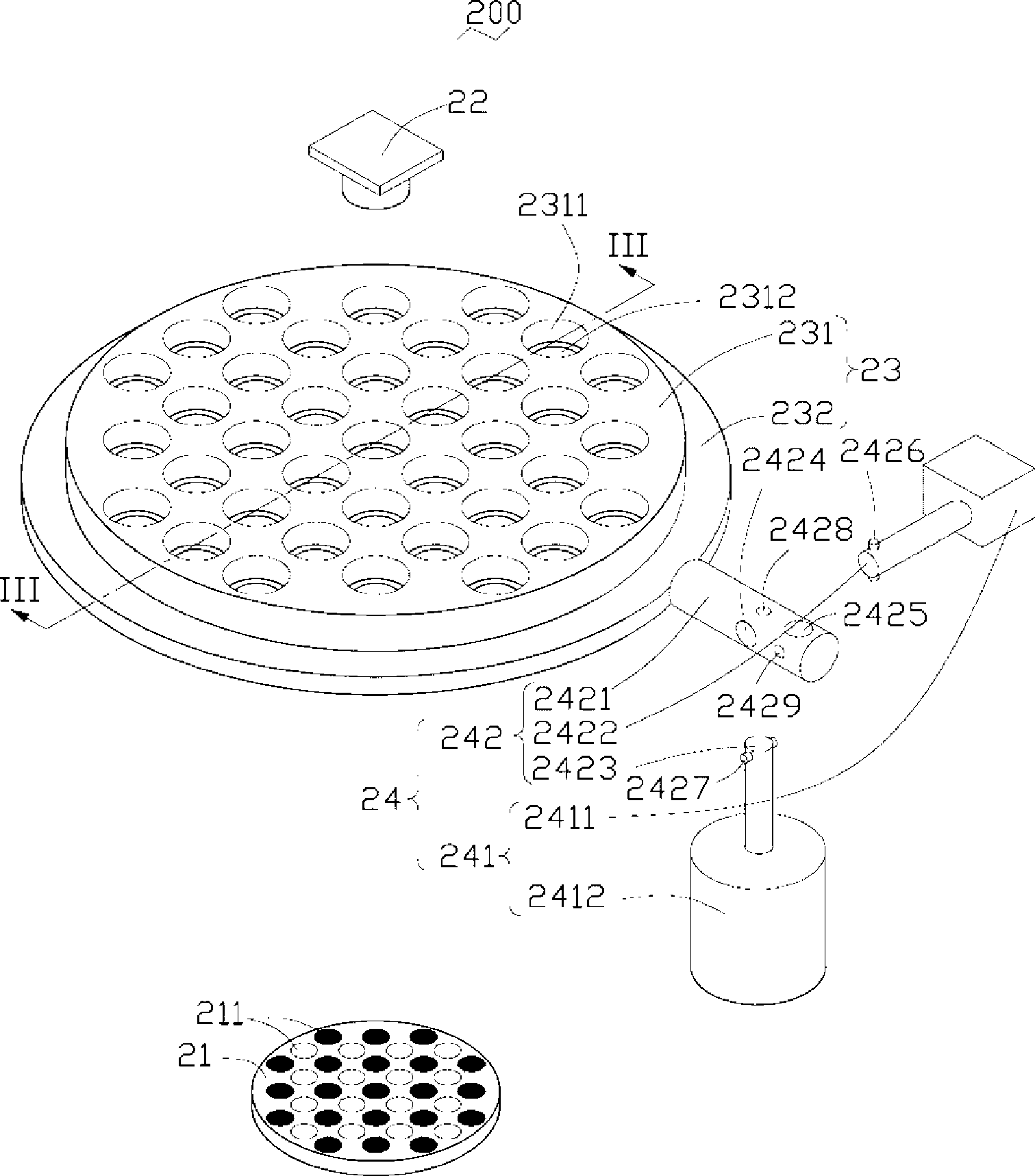
[0019] See figure 2 , Which is the modulation transfer function value measuring device 200 provided by the first embodiment of the technical solution, which includes a test board 21, an image sensor 22, a carrying device 23, and a driving device 24. The modulation transfer function value measuring device 200 is used to measure the modulation transfer function value of the lens.
[0020] The test board 21 has multiple areas with different brightness, for ease of description, figure 2 A plurality of patterns 211 indicate areas of different brightness. For the needs of subsequent measurement, a first test area and a second test area are defined on the test board 21. Both the first test area and the second test area have multiple light and dark patterns 211. For example, the patterns on the edge of the test board 21 are marked with 1, 2, 3, 4, 5, 6, 7 and 8, respectively, such as Figure 4A As shown, the first test area refers to a rectangular area surrounded by the four patterns 1, 3, 5, and 7 as the vertices, and the second test area refers to the rectangular area surrounded by the four patterns 2, 4, 6, and 8 as the vertices. The rectangular area. Thus, the first test area and the second test area partially overlap. In addition, the first test area can also be separated from the second test area, such as Figure 4B As shown, the test board 21' has a plurality of light and dark patterns 211', and the patterns on the edges thereof are respectively 1', 2', 3', 4', 5', 6', 7', 8', 9'and 10' mark, the first test area refers to the area surrounded by five patterns of 1', 2', 8', 9'and 10' as the vertices, and the second test area refers to the area surrounded by 3', 4', 5 The five patterns of', 6'and 7'are areas surrounded by vertices, so the first test area and the second test area are separated from each other without overlapping. In this embodiment, the first test area and the second test area are as follows Figure 4A Shown overlap each other. The test board 21 and the image sensor 22 are respectively located on opposite sides of the supporting device 23.
[0021] The image sensor 22 is used to sense the images formed on the image sensor 22 after the plurality of patterns 211 of the test board 21 are imaged through the lens to be tested. The image sensor 22 may be a charge-coupled image sensor or a complementary metal oxide semiconductor image sensor. Since the size of the test board 21 is large, which exceeds the sensing range of the image sensor 22, the image sensor 22 cannot sense all patterns of the test board 21 at one time. In this embodiment, the image sensor 22 can only sense the first test area surrounded by the four patterns 1, 3, 5, and 7 at a time, or the four patterns 2, 4, 6, and 8 as the apexes. Into the second test area.
[0022] Please refer to figure 2 and image 3 , The bearing device 23 includes a limiting device 231 and a bearing platform 232.
[0023] The limiting device 231 is used to fix the lens to be tested. The limiting device 231 has a circular shape with a plurality of first grooves 2311 on one surface, and a plurality of second grooves 2312 communicating with the first grooves 2311 on the other surface. The shape and size of the first groove 2311 match the shape and size of the lens to be tested, and the size of the second groove 2312 is slightly smaller than the size of the first groove 2311, that is, slightly smaller than the size of the lens to be tested Thus, a stepped through hole structure penetrating the opposite surfaces of the limiting device 231 is formed. The first groove 2311 and the second groove 2312 cooperate with each other to fix the lens to be tested. The position-limiting device 231 is arranged on the carrying platform 232, which is located on the same side of the carrying platform 232 as the image sensor 22 and is opposite to the image sensor 22.
[0024] The carrying platform 232 is provided with through holes 2321 penetrating through two opposite surfaces thereof. The size of the through hole 2321 is slightly smaller than the size of the limiting device 231, and the positions of all the first grooves 2311 in the limiting device 231 correspond to the area where the through hole 2321 is vertically projected by the limiting device 231. With this arrangement, the imaging light can pass through the second groove 2312 and the through hole 2321 without being blocked, so that the lens to be tested can image all the patterns on the test board 210. As a modification, the two opposite surfaces of the carrying platform 232 may also be provided with a plurality of through holes adapted to the shape and size of the second groove 2312, so that the imaging light can pass through the through holes without being blocked, so that The measuring lens realizes imaging of all patterns on the test board 21 at one time.
[0025] The driving device 24 is used to drive the bearing platform 232 so that it can drive the limiting device 231 to move parallel to the test board 21. The driving device 24 may be a commonly used driving device in the field. In this embodiment, the driving device 24 includes a driver 241 and a transmission member 242.
[0026]The driver 241 includes a first driver 2411 and a second driver 2412. The transmission member 242 includes a first transmission arm 2421, a second transmission arm 2422 and a third transmission arm 2423. The first driver 2411 may be a piezoelectric element or a motor, which is used to drive the second transmission arm 2422 of the transmission member 242 to move horizontally. The second driver 2412 is a motor for driving the third transmission arm 2423 of the transmission member 242 to rotate. The second transmission arm 2422 and the third transmission arm 2423 are respectively provided with a first elastic protrusion 2426 and a second elastic protrusion 2427. The first transmission arm 2421 is radially provided with a first limiting hole 2424 whose shape and size match the radial cross-sectional shape and size of the second transmission arm 2422, and a first limiting hole 2424 that matches the radial cross-sectional shape and size of the third transmission arm 2423. Two limiting holes 2425, a third limiting hole 2428 and a fourth limiting hole 2429 respectively adapted to the first elastic protrusion 2426 and the second elastic protrusion 2427. The third limiting hole 2428 and the first limiting hole 2424 pass through each other to form a cross hole for cooperating and fixing the second transmission arm 2422 to the first transmission arm 2421. The fourth limiting hole 2429 and the second limiting hole 2425 pass through each other to form another cross hole for fixing the third transmission arm 2423 to the first transmission arm 2421. The first transmission arm 2421 is arranged horizontally, one end of which is integrated with the bearing platform 232, and the other end thereof can be selectively connected to the second transmission arm 2422 arranged horizontally or the third transmission arm 2423 arranged vertically and horizontally. The second transmission arm 2422 is connected to the first driver 2411 and can move horizontally under the drive of the first driver 2411. The third transmission arm 2423 is connected to the second driver 2412 and can be rotated by the second driver 2412.
[0027] When the driving device 24 is used, the end of the second transmission arm 2422 that is not connected to the first driver 2411 can be inserted into the first limiting hole 2424 on the first transmission arm 2421, and the first elastic protrusion 2426 can pass through the Three limit holes 2428, so that the first transmission arm 2421 is sleeved to the second transmission arm 2422, so that the second transmission arm 2422 moves horizontally under the action of the first driver 2411, and at the same time drives the first transmission arm 2421 horizontally Move, thereby driving the carrying platform 232 and the limiting device 231 to move parallel to the test board 21. Or insert the end of the third transmission arm 2423 that is not connected to the second driver 2412 into the second limit hole 2425 on the first transmission arm 2421, and make the second elastic protrusion 2427 pass through the fourth limit hole 2429, In this way, the first transmission arm 2421 and the third transmission arm 2423 are sleeved into one body, so that the third transmission arm 2423 rotates under the action of the second driver 2412 while driving the bearing platform 232 to rotate parallel to the test board 21. Of course, according to specific needs, the carrying platform 232 and the limiting device 231 first move parallel to the test board 21 and then rotate parallel to the test board 21. Therefore, the first driver 2411 and the second driver 2412 are used in conjunction with the transmission member 242 to adjust the relative position of the carrying table 232 and the test board 21, so that the image sensor 22 can sense each pattern of different parts of the test board 21 211 The image formed by the lens to be tested.
[0028] When the modulation transfer function value measuring device 200 is used, multiple lenses to be tested need to be fixed to the first groove 2311 of the limiting device 231 respectively. Then the driver 241 of the driving device 24 drives the transmission member 242 to adjust the position of the carrier 232 relative to the test board 21, so that the lens to be tested can image all the patterns of the test board 21 at a time, and the image sensor 22 senses the first test board 21. After each pattern in the first test area and the second test area is imaged by the lens to be tested, the modulation transfer function value of the lens to be tested can be measured.
[0029] The modulation transfer function value measuring device 200 of this embodiment can measure the modulation transfer function values ​​of multiple lenses to be tested at one time. Now, taking one lens to be tested 300 among the plurality of lenses to be tested as an example, the method for measuring the value of the modulation transfer function of the lens by the measuring device 200 for the modulation transfer function value will be described in detail. The method mainly includes the following steps:
[0030] Step 1: Fix the lens 300 to be tested on the limiting device 231, use the image sensor 22 to sense the image formed by the first test area of ​​the test board 21 through the lens 300 to be tested, and record the first maximum brightness and the first maximum brightness of the image. A minimum brightness.
[0031] Specifically, during the test, the selection of the first maximum brightness value and the first minimum brightness value is performed in the following manner.
[0032] A pixel of the image sensor 22 is selected, and the selected pixel senses the brightness value of the first test area, obtains the first maximum brightness and the first minimum brightness, and records them.
[0033] If in every three consecutive patterns, the brightness value of the pattern at the middle position is greater than the brightness value of the pattern at the front and back positions, then the brightness value of the pattern at the middle position is the first maximum brightness of the image sensed by the selected pixel ; If the brightness value of the pattern at the middle position is less than the brightness value of the pattern at its front and back positions, the brightness value of the pattern at the middle position is the first minimum brightness of the image sensed by the selected pixel.
[0034] Step 2: Adjust the relative position of the carrying device 23 and the test board 21 through the driving device 24, use the image sensor 22 to sense the image of the second test area of ​​the test board 21 through the lens 300 to be tested, and obtain the image brightness The second maximum brightness and the second minimum brightness.
[0035] The position of the carrying device 23 relative to the test board 21 can be adjusted by the driver 241 of the driving device 24 driving the transmission member 242 to drive the carrying table 232 and the lens 300 to be tested to move. The movement is the movement or rotation of the carrying platform 232 parallel to the test board 21, but the image sensor 220 should be able to sense the image of the second test area through the lens 300 to be tested. Specifically, when the first pattern overlaps the second pattern, such as Figure 5A As shown, the third transmission arm 2423 and the first transmission arm 2421 should be connected, and the second driver 2412 should be activated to make the carrying table 232 and the lens to be tested 300 rotate parallel to the test board 21, and then as shown Figure 5B As shown, disconnect the third transmission arm 2423 and the first transmission arm 2421, and then connect the second transmission arm 2422 and the first transmission arm 2411, and then start the first driver 2411, so that the bearing platform 232, the limit device 231 and The lens 300 to be tested moves parallel to the test board 21. When the first pattern and the second pattern are spaced apart, the carrier 232, the limiting device 231 and the lens 300 to be tested can be moved parallel to the test board 21 under the driving of the first driver 2411. In this embodiment, since the first test area is partially overlapped with the second test area, the carrier 232 and the lens to be tested 300 should be driven by the second driver 2412 to first rotate a certain angle parallel to the test board 21, and then The translation is performed under the driving of the first driver 2411, so that the image sensor 22 can sense the image formed by the second test area through the lens 300 to be tested. The effect diagram is shown in FIG. 6.
[0036] Record the brightness value of the second test area sensed by the selected pixels of the image sensor 22, and determine the second maximum brightness value and the second brightness according to the same method of determining the first maximum brightness value and the first minimum brightness value described above Minimum value.
[0037] Step 3: Compare the first maximum value of brightness with the second maximum value of brightness, and the first minimum value of brightness with the second minimum value of brightness, to obtain the maximum and minimum values ​​of brightness, thereby calculating the modulation transfer function value of the lens 300 to be tested .
[0038] According to the maximum and minimum brightness values ​​obtained by comparing the first brightness maximum value and the second brightness maximum value and the first brightness minimum value and the second brightness minimum value, the formula MTF=(I max -I min )/(I max +I min ) Calculate the modulation transfer function of the lens 300 to be tested. Where I max Is the maximum value of the brightness of the pattern sensed by the selected pixel of the image sensor 22, I min This is the minimum value of the brightness of the pattern sensed by the pixels of the image sensor 22.
[0039] After the image sensor 22 images all the patterns 211 through the lens 300 to be tested, the first driver 2411 and the second driver 2412 are operated according to the aforementioned method to make the carrier 232 and the lens 300 to be tested move or rotate parallel to the test board 21, The other lens 300 to be tested can just image all the patterns of the test board 21 at one time, and then the other lens 300 to be tested is measured according to the aforementioned method of measuring the modulation transfer function value.
[0040] See Figure 7 , Which is a schematic diagram of a modulation transfer function value measuring device 400 provided by the second embodiment of the technical solution. The difference from the measuring device 200 is that the transmission member 342 of the measuring device 400 is disposed on the central axis of the bearing platform 332, and the limiting device 331 is provided with a plurality of through holes that are the same as the stepped through holes of the limiting device 231. All stepped through holes are located on the circumference centered on the transmission member 342 to accommodate the lens to be tested.
[0041] When using the measuring device 400, such as Figure 8 As shown, the relative positional relationship between the lens 500 to be tested and the image sensor 32 and the test board 31 is adjusted so that the lens 500 to be tested can image all the images on the test board 31 at one time and is located in the sensing area of ​​the image sensor 32 . The driver 341 is operated to rotate the transmission member 342, so that the carrying platform 332 and the limiting device 331 rotate around the transmission member 342. At the same time, the lens 500 to be tested placed in each stepped through hole of the limiting device 331 is rotated. In this way, through the rotation of the lens 500 to be tested, the image sensor 32 can respectively sense the images formed by the patterns of different parts of the test board through the lens to be tested. The rotation of the lens 500 to be tested can be achieved by setting a planetary gear, that is, the transmission member 342 is connected with the planetary gear, so that the driver 341 drives the transmission member 342, and the transmission member 342 drives the planetary gear to rotate.
[0042] It is understandable that the pattern of the test board can be an array including a plurality of light and dark stripes arranged at intervals, or two of the stripe arrays, and the light and dark stripes of the two stripe arrays intersect.
[0043] As a modification, a driver connected to the image sensor can also be provided to move the image sensor along the optical axis of the lens to be tested to obtain the best image of the pattern passing through the lens to be tested.
[0044] In addition, those skilled in the art can also make other changes within the spirit of the present invention, such as appropriately changing the structure and type of the drive device, the number of drives, the positional relationship between the drive device and the carrier, and the shape and distribution of the pattern of the test board. . These changes made in accordance with the spirit of the present invention should all be included in the scope of protection claimed by the present invention.

PUM

no PUM

Description & Claims & Application Information

We can also present the details of the Description, Claims and Application information to help users get a comprehensive understanding of the technical details of the patent, such as background art, summary of invention, brief description of drawings, description of embodiments, and other original content. On the other hand, users can also determine the specific scope of protection of the technology through the list of claims; as well as understand the changes in the life cycle of the technology with the presentation of the patent timeline. Login to view more.

Similar technology patents

Installation and adjustment method of infrared lenses

ActiveCN102998767AHigh-precision adjustmentHigh measurement accuracyMountingsCamera lensOptical path
Owner:BEIJING RES INST OF SPATIAL MECHANICAL & ELECTRICAL TECH

Classification and recommendation of technical efficacy words

  • Improve detection efficiency
  • High measurement accuracy

Materials real-time detection and foreign body eliminating system based on machine vision

InactiveCN101176872AImprove detection efficiencyImprove image quality and accuracy of material detection and foreign object recognitionCharacter and pattern recognitionSortingLight sourceImage identification
Owner:SOUTH CHINA UNIV OF TECH

Screw rotor type surface profile error measurement instrument

ActiveCN102538700AAvoiding Probe Radius Compensation ProblemsHigh measurement accuracyUsing optical meansEngineeringHeadstock
Owner:HEFEI UNIV OF TECH

High performance direct shearing apparatus for large contact surfaces

ActiveCN102207436AHigh measurement accuracyLarge cut surface sizeUsing mechanical meansMaterial strength using steady shearing forcesShearing deformationNormal displacement
Owner:NANJING HYDRAULIC RES INST

Method for analyzing components of iron ore by using X-ray fluorescence spectrum

InactiveCN101526488AHigh measurement accuracySimplify measurement procedures and timeMaterial analysis using wave/particle radiationCalibration curveSoft x ray
Owner:HUNAN VALIN XIANGTAN IRON & STEEL CO LTD
Why Eureka
Try Eureka