Check patentability & draft patents in minutes with Patsnap Eureka AI!

Stacked packaging structure

A packaging structure, stacking technology, applied in the direction of semiconductor/solid-state device components, semiconductor devices, electrical components, etc., can solve the problem that the single-chip packaging technology cannot meet the demand and other problems, achieve a small number, a large area, and overcome the cold junction. Effect

Inactive Publication Date: 2009-06-24
POWERTECH TECHNOLOGY
View PDF0 Cites 2 Cited by
  • Summary
  • Abstract
  • Description
  • Claims
  • Application Information

AI Technical Summary

Problems solved by technology

[0002] Under the trend of thin, light, small and multi-functional, the traditional single-chip packaging technology has gradually failed to meet the demand

Method used


Image

  • Stacked packaging structure
  • Stacked packaging structure
  • Stacked packaging structure

Examples


Embodiment Construction

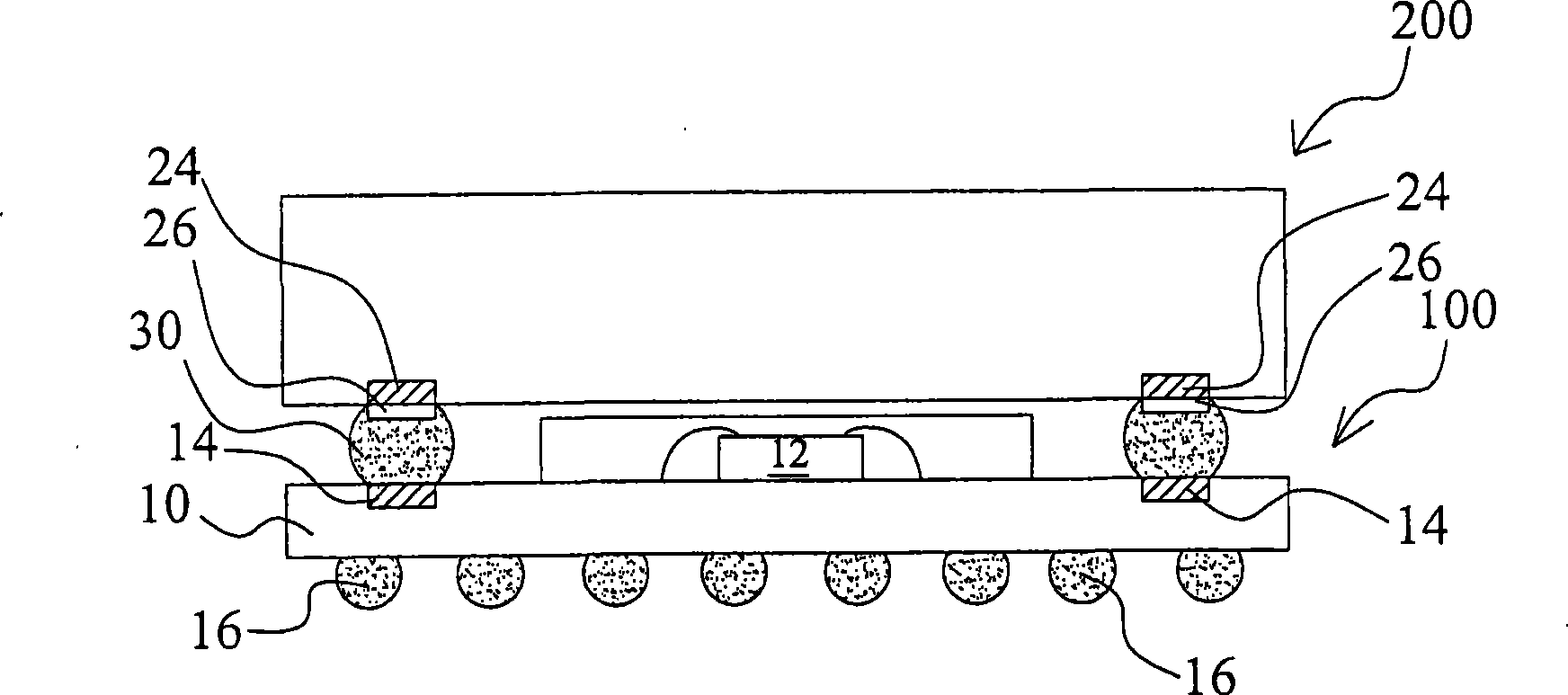
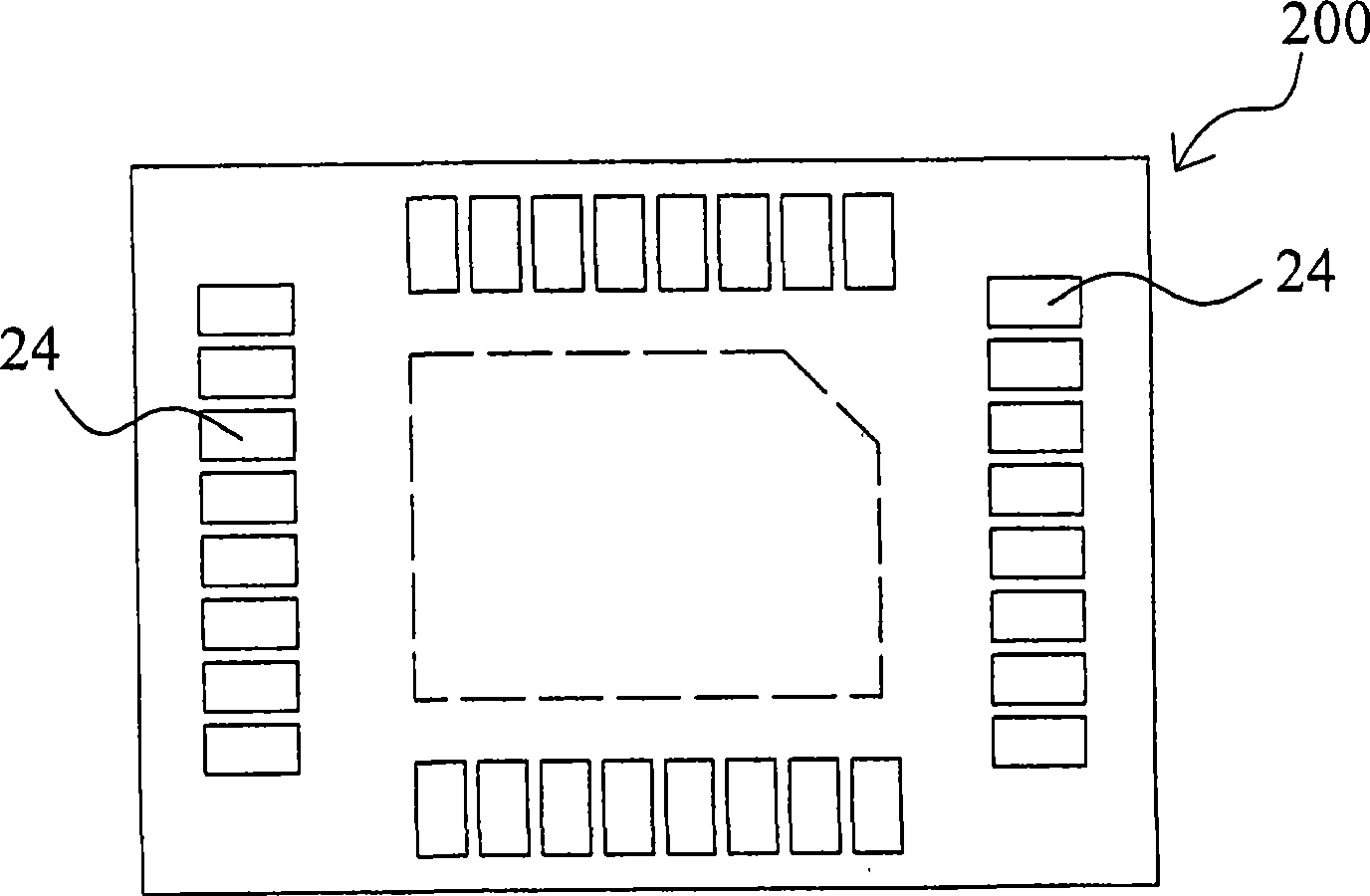
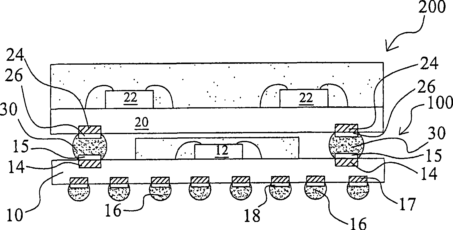
[0027] figure 1 Shown is a schematic diagram according to an embodiment of the present invention. In this embodiment, the package-on-package structure includes: a first package body 100 ; a plurality of second conductive solder balls 30 ; and a second package body 200 . The second package body 100 is stacked on the first package body 100 by using the second conductive solder balls 30 .

[0028] Such as figure 1 As shown, the first package 100 is a ball grid array package. The first package 100 includes a first substrate 10 having an upper surface and a lower surface. At least one first chip 12 is disposed on the upper surface of the first substrate 10 . A plurality of first conductive pads 14 are disposed and exposed on the upper surface of the first substrate 10 ; and a plurality of first conductive solder balls 16 are disposed on the lower surface of the first substrate. The second conductive solder ball 30 is disposed on the first conductive pad 14 .

[0029] In additi...


PUM


Abstract

The invention relates to a stacked-type package structure, comprising a second packaging body stacked on a first packaging body through a plurality of second conductive weld beads. The first packaging body is a ball grid array packaging body and comprises a first substrate; the first substrate is provided with an upper surface and a lower surface; at least a first chip is arranged on the upper surface of the first substrate; a plurality of first conductive connection pads are arranged on the upper surface of the first substrate; and a plurality of first conductive weld beads are arranged on the lower surface of the first substrate. The second conductive weld beads are arranged on the first conductive connection pads. In addition, the second packaging body is a square flat pin-free packaging body. A plurality of second conductive connection pads are rectangular and are arranged around the circumferential edge of the bottom part of the second packaging body. A plurality of second conductive welding parts are arranged on the second conductive connection pads and protruded from the lower surface of the second packaging body; and the second conductive weld beads are connected with the second conductive welding parts.

Description

technical field [0001] The invention relates to chip packaging technology, in particular to a stacked packaging structure. Background technique [0002] With the trend of light, thin, small and multi-functional, the traditional single-chip packaging technology has gradually been unable to meet the demand. Therefore, using various stacked packaging methods to reduce the packaging volume and packaging thickness of chips with different functions is the current development focus of packaging technology. Package on Package (POP) is one of the packaging technologies. [0003] Stacked packaging is to stack two independently packaged packages with process technology. Since the two packages are respectively packaged and tested, they are stacked and adhered to each other. In existing stacked packages, two packages are electrically connected by solder. However, how to overcome the cold junction problem during warpage and how to improve the yield of stacked packaging products is sti...

Claims


Application Information

Patent Timeline
Patent Type & Authority Applications(China)
IPC IPC(8): H01L25/00H01L25/065H01L23/488
CPCH01L2924/15311H01L2924/181H01L2224/32145H01L2224/48091H01L2224/48227H01L2224/4824H01L2224/73215H01L2224/73265H01L2924/00014H01L2924/00012H01L2924/00
Inventor 陈建宏
Owner POWERTECH TECHNOLOGY
Features
  • R&D
  • Intellectual Property
  • Life Sciences
  • Materials
  • Tech Scout
  • Unparalleled Data Quality
  • Higher Quality Content
  • 60% Fewer Hallucinations
Learn More