Automatic flaw detection device and method for substrate laser repairing device

A technology of laser repair and defect detection, which is applied in the fields of optics, nonlinear optics, semiconductor/solid-state device testing/measurement, etc., can solve the problems of manpower consumption, reduction, slow speed, etc., save time and trouble, and solve the problem of misjudgment , The effect of low probability of missing defects

Inactive Publication Date: 2009-07-01
IND TECH RES INST
View PDF0 Cites 14 Cited by
  • Summary
  • Abstract
  • Description
  • Claims
  • Application Information

AI Technical Summary

Problems solved by technology

However, the electric test can only detect which line has a defect near it, and cannot accurately find out the exact defect coordinates
Taking a 1000mm long line (gate / source line) as an example, it takes at least 5 minutes to complete the inspection with human eyes (taking 5um pixel resolution as an example), which is slow and labor-intensive, and it is easy to cause damage to the eyes of the inspector. fatigue and vision loss
Therefore, there are still deficiencies in the automatic defect detection device of the existing substrate laser repair machine and need to be improved

Method used


Image

  • Automatic flaw detection device and method for substrate laser repairing device
  • Automatic flaw detection device and method for substrate laser repairing device
  • Automatic flaw detection device and method for substrate laser repairing device

Examples


Embodiment Construction

[0047] While the invention will be fully described with reference to the accompanying drawings, which contain preferred embodiments of the invention, it is before proceeding to this description that it is understood that those skilled in the art may modify the invention described herein while still obtaining the benefits of the invention. Therefore, it should be understood that the following description is a broad disclosure for those skilled in the art, and its content is not intended to limit the present invention.

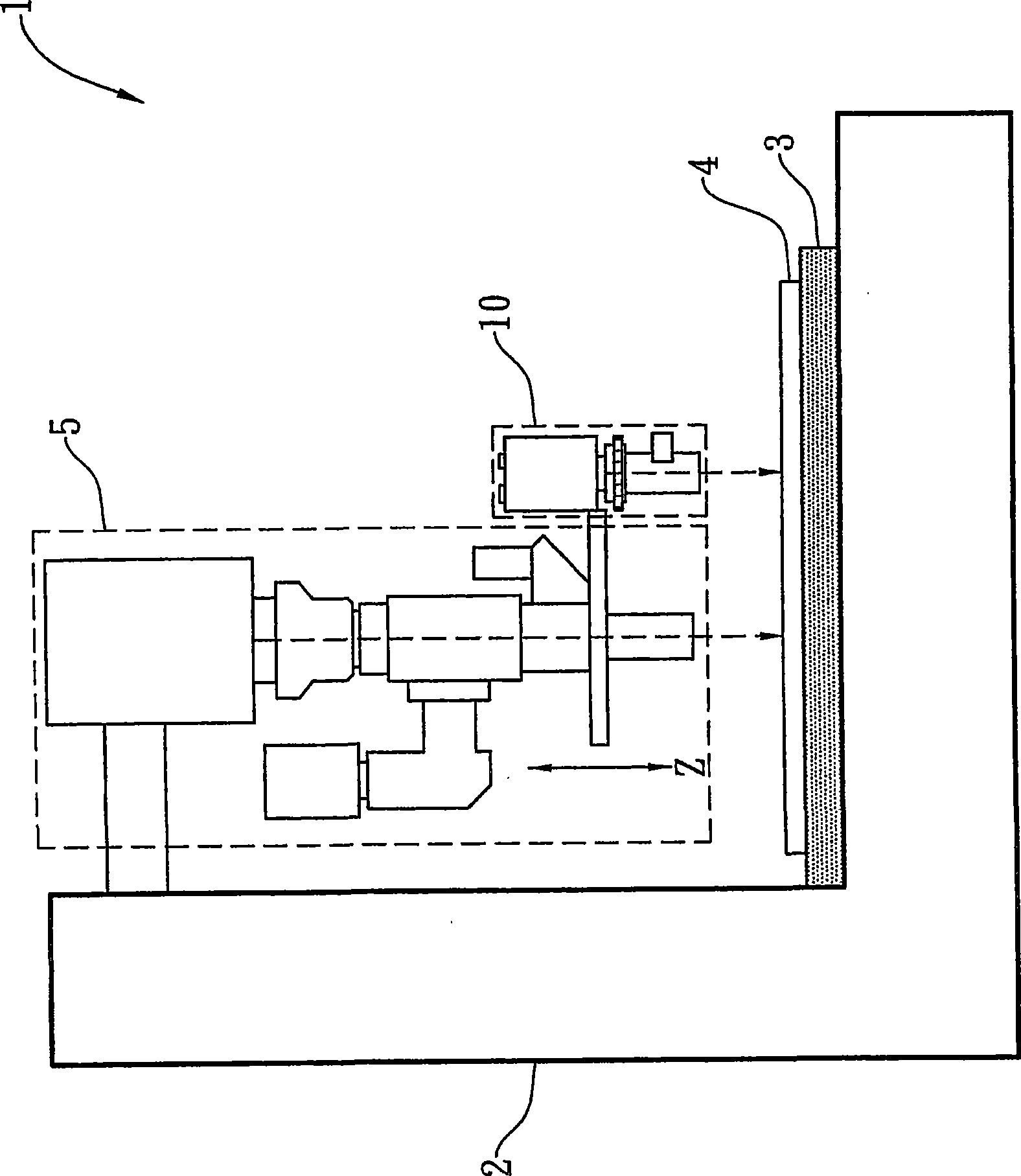
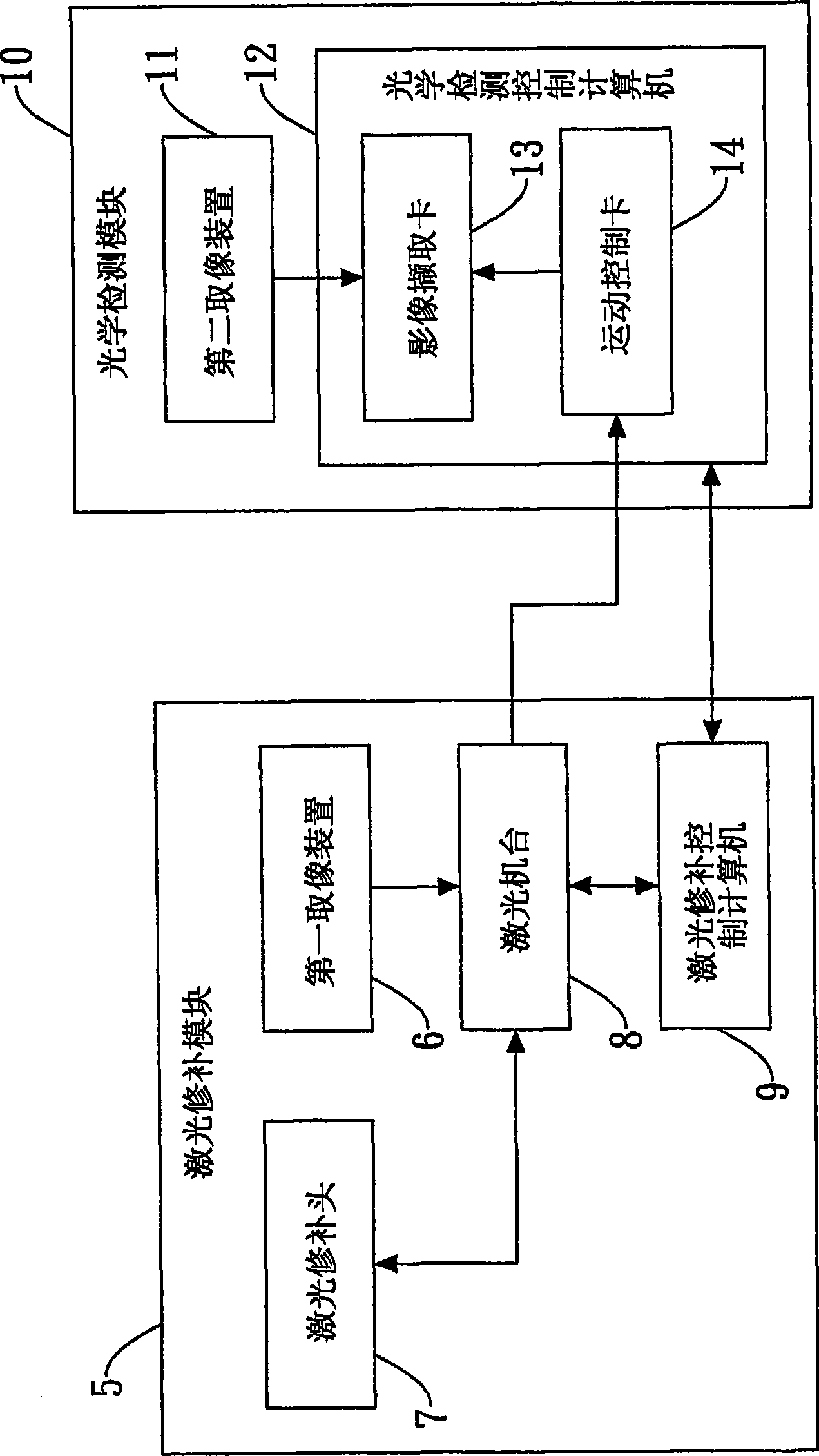
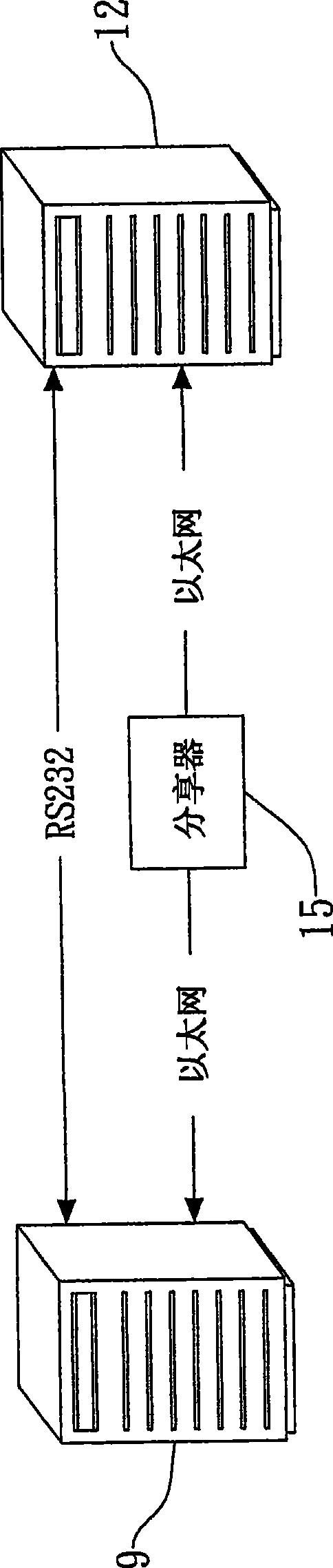
[0048] see figure 1 and figure 2 A schematic diagram and a block diagram of the automatic defect detection device 1 of the substrate laser repairing machine of the present invention are shown respectively. The automatic defect detection device 1 of the substrate laser repairing machine of the present invention comprises a machine base 2; a substrate carrying platform 3 set on the machine base 2; a substrate 4 carried on the substrate supporting platform 3; a l...


PUM


Abstract

The invention relates to a base-plate laser-repairing machine automatic flaw checkout gear and method. After a base-plate is electrically tested, according to the results of the electrical test, a second view-finding device of an optical examination module replaces eyes to high-speed view-find defect lines and detect out the defects through an image detection mode of a laser-repairing module, which is convenient for subsequent laser-repairing movements.

Description

technical field [0001] The invention relates to an automatic defect detection device and method for a substrate laser repair machine, in particular to an automatic defect detection device and method for a substrate laser repair machine combined with a laser repair module and an optical detection module. Background technique [0002] After the integrated circuit chip is manufactured, the integrated circuit still needs many complicated process steps before the integrated circuit can be used by users. The many complicated process steps include at least several typical process steps such as chip testing, chip packaging, and final testing. [0003] When testing before semiconductor components are packaged, the chip is first selected and tested on the chip, and the bad memory units measured on the chip of the chip are made into repair data, and then the chip is placed in the laser machine, and the data is used for processing. Laser repair enables the defective chips detected in t...

Claims


Application Information

Patent Timeline
Patent Type & Authority Applications(China)
IPC IPC(8): H01L21/66G02F1/13
Inventor 洪朝阳郑智杰吕尚杰张俊隆
Owner IND TECH RES INST
Why Eureka
Try Eureka