Semiconductor memory device and method for fabricating the same

A technology for storage devices and manufacturing methods, applied in semiconductor/solid-state device manufacturing, semiconductor devices, information storage, etc., can solve problems such as data disappearance and chip ID can no longer be read

Inactive Publication Date: 2009-07-15
PANASONIC CORP
View PDF1 Cites 5 Cited by
  • Summary
  • Abstract
  • Description
  • Claims
  • Application Information

AI Technical Summary

Problems solved by technology

As a result, the chip ID or chip-specific information can no longer be read out, so that the data disappears in a substantial sense

Method used


Image

  • Semiconductor memory device and method for fabricating the same
  • Semiconductor memory device and method for fabricating the same
  • Semiconductor memory device and method for fabricating the same

Examples


no. 1 approach

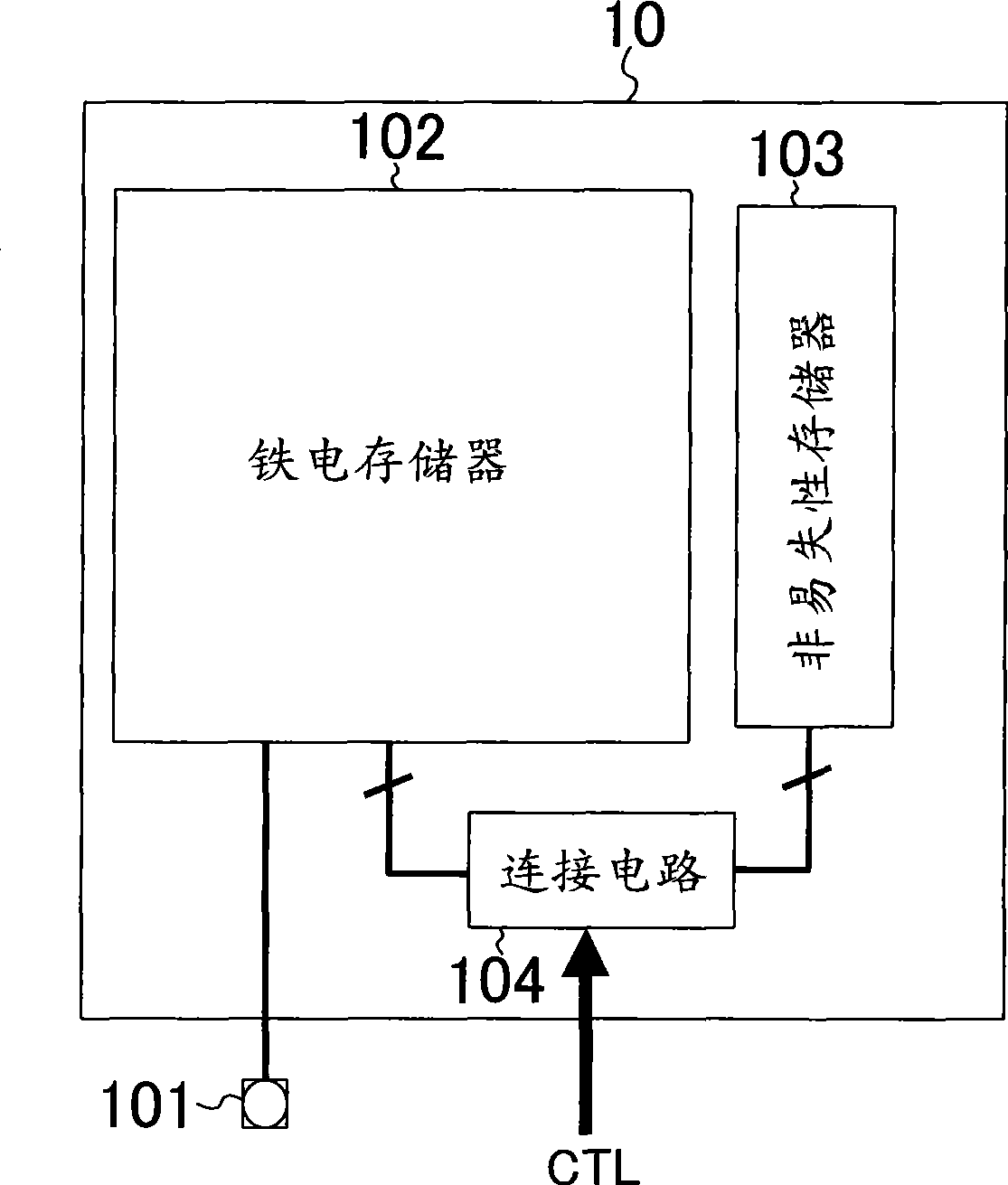
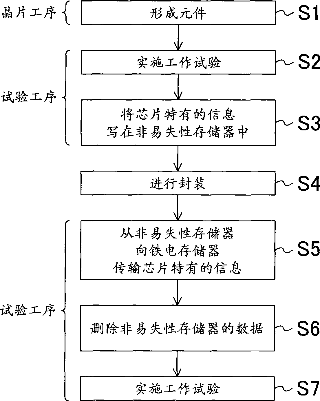
[0020] figure 1 The structure of the semiconductor storage device (hereinafter, this semiconductor storage device will also be simply referred to as a "chip") according to the first embodiment is shown. In the chip 10 according to the present embodiment, the terminal 101 is a terminal for reading or writing data to the ferroelectric memory 102 . The nonvolatile memory 103 is a memory whose ability to hold data at high temperatures is higher than that of the ferroelectric memory 102 . Specifically, a fuse that can be physically cut (physical fuse), a fuse that can be cut electrically (eFUSE: Electronic Fuse), or a nonvolatile memory composed of CMOS (Complementary Metal Oxide Semiconductor) transistors (Complementary Metal Oxide Semiconductor) can be used. Semiconductor nonvolatile memory) and the like constitute the nonvolatile memory 103, and the nonvolatile memory 103 can also be constituted by combining the above-mentioned components according to circumstances. The connec...

no. 2 approach

[0027] image 3 The structure of the semiconductor memory device according to the second embodiment is shown. The chip 10 according to this embodiment has a configuration in which a terminal 105 capable of accessing a nonvolatile memory 103 is added to the semiconductor memory device according to the first embodiment. According to this embodiment, the data written in the nonvolatile memory 103 can be directly read from the terminal 105 without going through the ferroelectric memory 102, and can be confirmed. In addition, when the nonvolatile memory 103 includes an electronic fuse or a complementary metal oxide semiconductor nonvolatile memory, it is possible to directly input the data to be written to the nonvolatile memory 103 from the terminal 105 without passing through the ferroelectric memory 102 . The data.

no. 3 approach

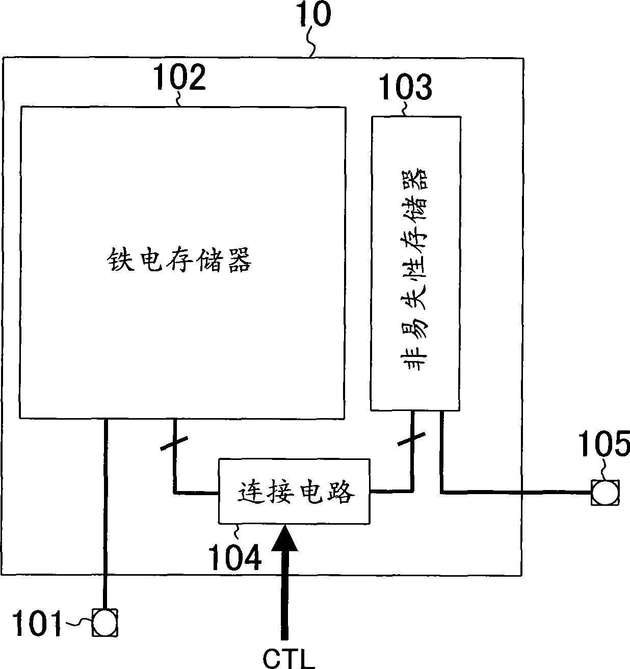
[0029] Figure 4The structure of the semiconductor memory device according to the third embodiment is shown. The chip 10 according to this embodiment has a structure in which the terminal 105 in the semiconductor memory device according to the second embodiment is not connected to the nonvolatile memory 103 but is connected to the connection circuit 104 . The connection circuit 104 switches the connection state between the ferroelectric memory 102 and the nonvolatile memory 103 and the connection state between the nonvolatile memory 103 and the terminal 106 . In the second embodiment, a data bus for interconnecting the nonvolatile memory 103 and the terminals 105 is required, but such a data bus is not required in the present embodiment. Therefore, according to the present embodiment, the chip area can be reduced to an area smaller than that of the second embodiment.


PUM


Abstract

The present invention discloses a semiconductor memory device and a method for fabricating the same. The semiconductor memory device (10) including a ferroelectric memory (102) includes: a nonvolatile memory (103) having higher data retention capability under high temperature than the ferroelectric memory (102); and a connection circuit (104) for switching between connection and disconnection of the ferroelectric memory and the nonvolatile memory (103). The ferroelectric memory (102) receives, through the connection circuit (104), at least part of data which is unique to the device and which has been written into the nonvolatile memory (103), and retains the received data. Conventionally loss of the data written into a ferroelectric memory may be prevented due to heat treatment in process of fabricating the ferroelectric memory.

Description

technical field [0001] The invention relates to a semiconductor storage device including a ferroelectric memory, in particular to a data protection technology of the ferroelectric memory during the manufacturing process. Background technique [0002] The manufacturing process of a semiconductor storage device including a ferroelectric memory is roughly as follows: First, elements such as a ferroelectric memory and a control circuit are formed in a wafer; after the elements are formed, an operation test is carried out while maintaining the shape of the wafer; Finally, chip-specific information such as the chip ID (identifier) ​​is written into the specified area in the ferroelectric memory; after the chip-specific information is written, each chip is enclosed in a package for packaging; after packaging, the work test. Thus, the semiconductor memory device (ferroelectric memory chip) including the ferroelectric memory is manufactured. [0003] A problem here is that the ferr...

Claims


Application Information

Patent Timeline
Patent Type & Authority Applications(China)
IPC IPC(8): G11C11/22H01L21/00
CPCH01L27/11592G11C11/22H01L27/11509Y10T29/49002H10B53/40H10B51/40
Inventor 中尾良昭五宝靖岩成俊一村久木康夫松浦正则
Owner PANASONIC CORP
Why Eureka
Try Eureka