Solid state imaging device and manufacturing method thereof

A technology of solid-state imaging and manufacturing methods, which is applied in the direction of electric solid-state devices, radiation control devices, semiconductor devices, etc., and can solve problems such as performance degradation of optical sensors, reduction of conduction current, and degradation of transistor characteristics.

Inactive Publication Date: 2013-06-05
KK TOSHIBA
View PDF4 Cites 1 Cited by
  • Summary
  • Abstract
  • Description
  • Claims
  • Application Information

AI Technical Summary

Problems solved by technology

Thus, an increase in threshold voltage and / or a decrease in on-current are caused, resulting in deterioration of transistor characteristics as
As a result, even if the transfer transistor is turned on, the charge accumulated in the charge accumulation diffusion layer of the photodiode is difficult to transfer to the floating diffusion layer, so the performance as a photosensor deteriorates.

Method used


Image

  • Solid state imaging device and manufacturing method thereof
  • Solid state imaging device and manufacturing method thereof
  • Solid state imaging device and manufacturing method thereof

Examples


no. 1 Embodiment approach )

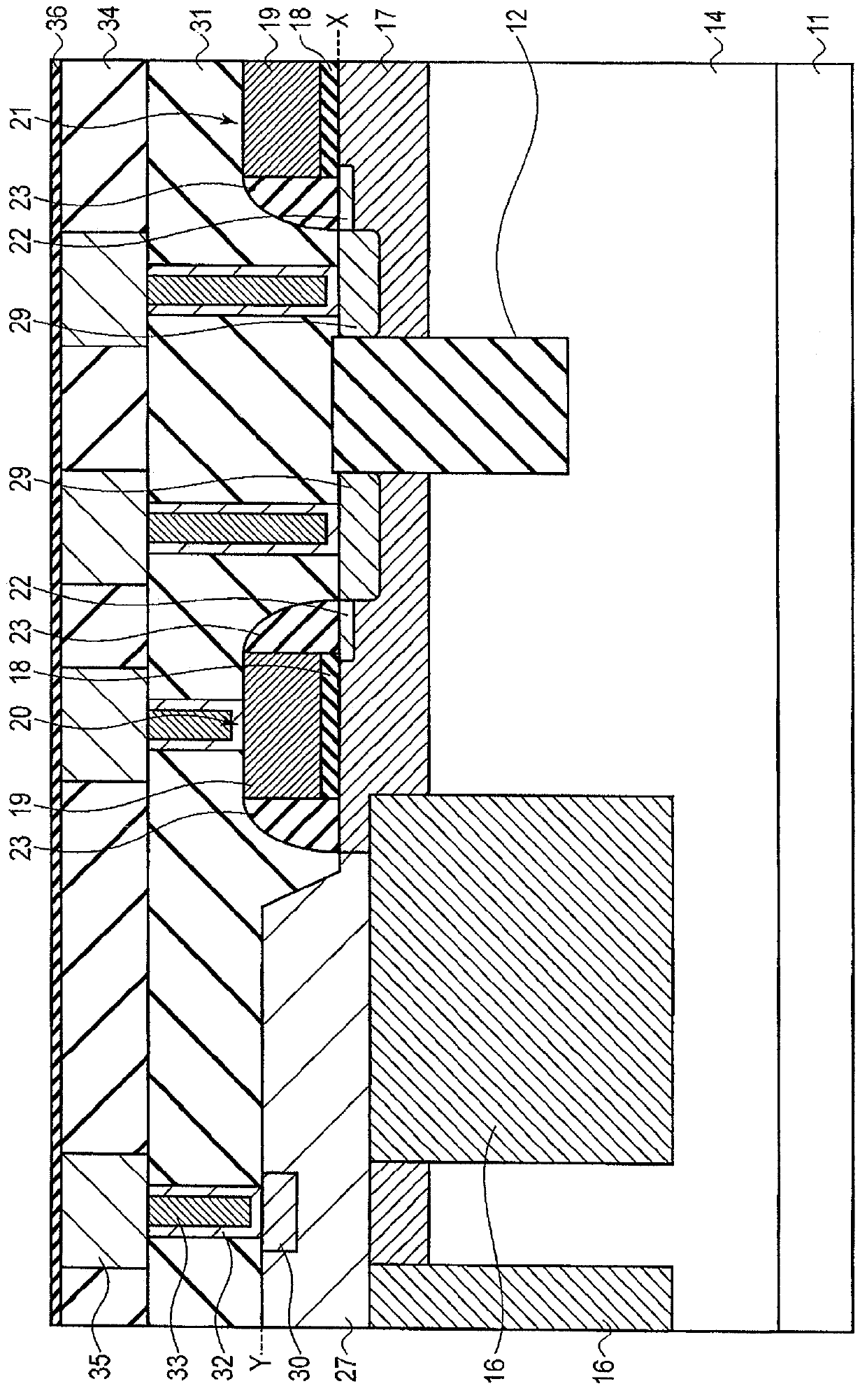
[0035] The solid-state imaging device according to the first embodiment includes a CMOS sensor. figure 1 It is a cross-sectional view of the solid-state imaging device according to the first embodiment.

[0036] A solid-state imaging device includes a pixel array including a plurality of pixels. Each pixel includes: a photoelectric conversion element (photodiode) 16 that converts incident light into charges; a transfer transistor 20 that transfers the charges accumulated in the photodiode 16 to the floating diffusion layer 29; and a voltage of the floating diffusion layer 29 as a signal. Level output amplifier transistor 21 and so on.

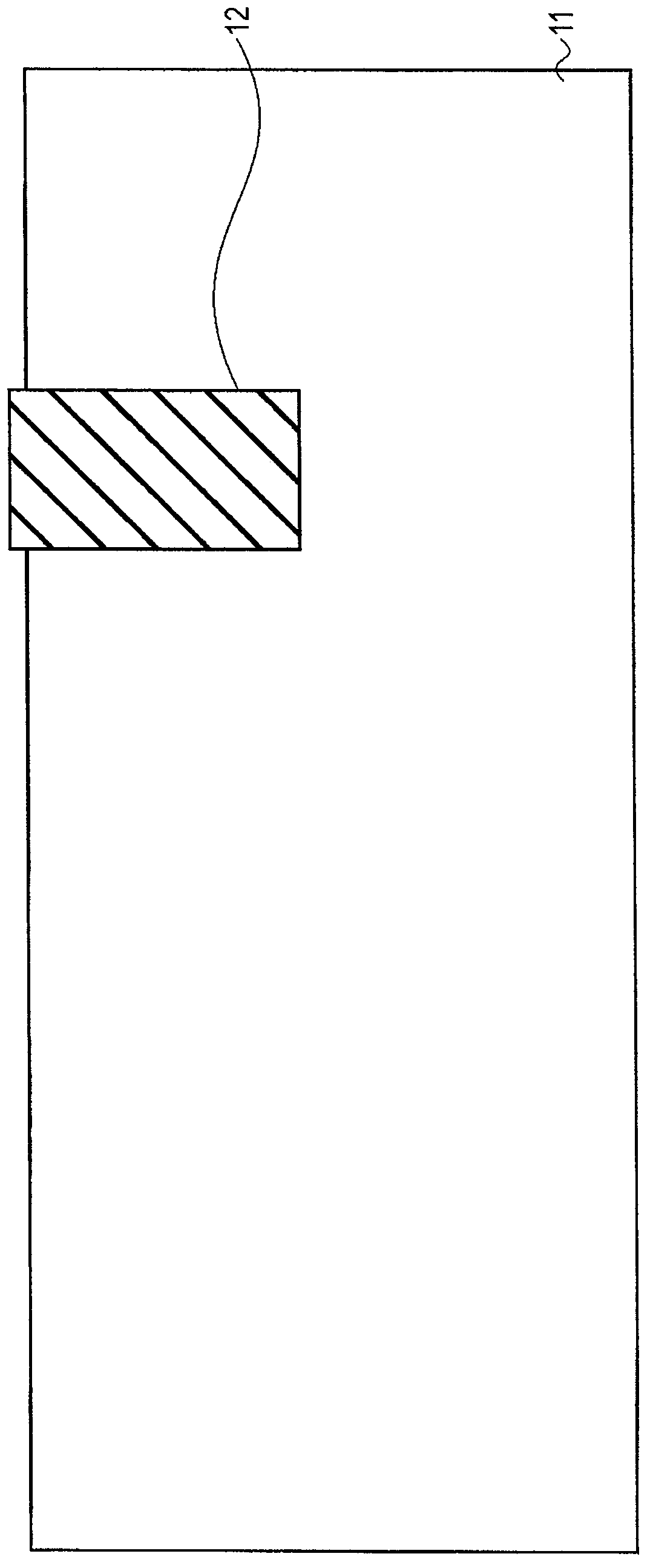
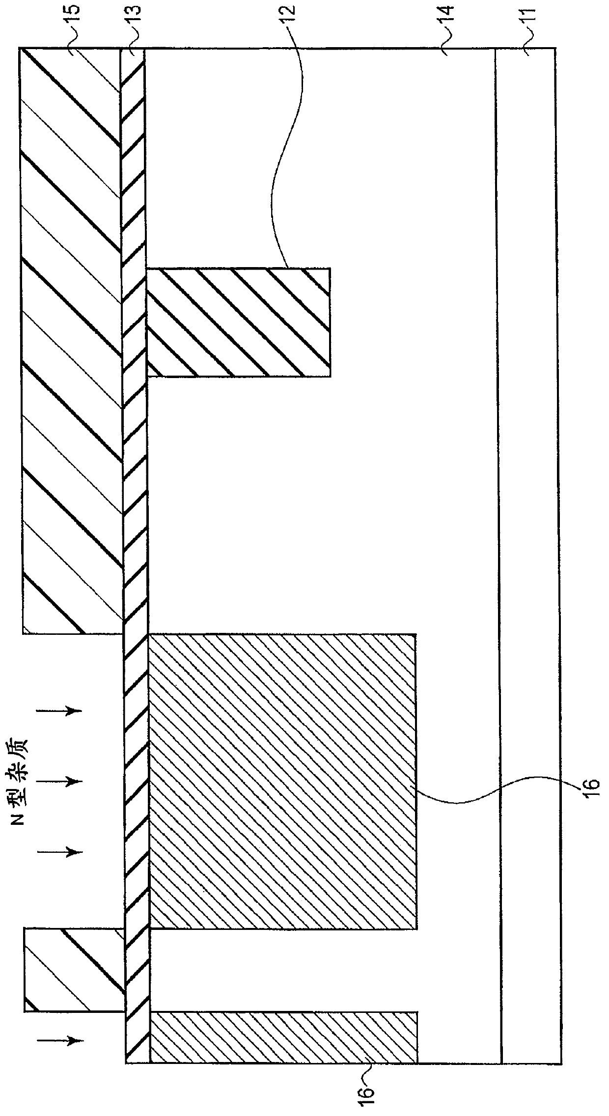
[0037] figure 1 , the symbol “X” represents the position of the top surface of the semiconductor substrate (eg silicon substrate) 11 . Inside the silicon substrate 11 , a separation layer 14 is provided for electrically separating adjacent photodiodes 16 . The separation layer 14 includes a P-type semiconductor layer. In the surface region...

no. 2 Embodiment approach )

[0068] In the second embodiment, as the semiconductor layer constituting the shield layer, the same semiconductor material as that of the semiconductor layer constituting the gate electrode of the MOSFET is used. Furthermore, simultaneously with the step of forming the semiconductor layer for the gate electrode, the semiconductor layer for the shield layer is formed.

[0069] Figure 14 It is a cross-sectional view of the solid-state imaging device of the second embodiment. Similar to the first embodiment, an embedded photodiode 16 is provided in the silicon substrate 11 . That is, the top surface of the photodiode 16 is lower than the top surface X of the silicon substrate 11 . A shielding layer 27 is provided on the photodiode 16 . The top surface Y of the shield layer 27 is higher than the top surface X of the silicon substrate 11 . In addition, as the semiconductor layer constituting the shield layer 27 , the same semiconductor material as the semiconductor layer const...


PUM


Abstract

The invention provides a solid state imaging device capable of accurately reading electric charge accumulated in a photodiode and a manufacturing method thereof. The solid state imaging device provided by an embodiment comprises a semiconductor substrate, a photodiode which is disposed in the semiconductor substrate and is provided with a first conductive type semiconductor layer, a shielding layer which is disposed on the above photodiode and contains a second conductive type semiconductor layer in the upper portion or the whole of the shielding layer; and a transmission transistor which is disposed on the semiconductor substrate and transmits the electric charge accumulated in the photodiode to a floating diffusion layer. The top surface of the shielding layer is higher than that of the semiconductor substrate.

Description

[0001] This application enjoys the priority of Japanese Patent Application No. 2011-253710 filed on November 21, 2011, and the entire content of the Japanese Patent Application is cited in this application. technical field [0002] Embodiments of the present invention relate to a solid-state imaging device and a method of manufacturing the same. Background technique [0003] In recent years, the demand for imaging parts of mobile phones has increased rapidly. In addition, there is a strong demand for higher image quality and higher performance of CMOS sensors, especially pixel miniaturization in order to meet the demand for larger pixels (pixels). Along with this demand for higher image quality, it is required to further reduce dark noise generated in pixels and / or defective pixels recognized as white spots on the screen called white spots. This is due to the occurrence of dark current and / or leakage current due to an interface level formed at the interface of the silicon s...

Claims


Application Information

Patent Timeline
IPC IPC(8): H01L27/146H04N5/335
CPCH01L31/18H01L27/1461H01L31/02H01L27/14623
Inventor 吉田毅
Owner KK TOSHIBA
Why Eureka
Try Eureka