
Imaging device

An imaging device and carrier technology, applied in radiation control devices, etc., can solve problems such as difficulty in miniaturization of imaging devices

Inactive Publication Date: 2007-08-08
SANYO ELECTRIC CO LTD
View PDF0 Cites 1 Cited by
  • Summary
  • Abstract
  • Description
  • Claims
  • Application Information

AI Technical Summary

Problems solved by technology

[0009] However, in the conventional CCD image sensor shown in FIG. 12, there is a disadvantage in that, in order to transfer electrons (carriers) transferred from the photodiode 108 to the multiplication region for multiplying electrons, namely Charge storage well transfer requires pixel separation barriers, temporary storage wells, and three gate electrodes 103-105 for forming charge transfer barriers respectively
Therefore, there is a problem that miniaturization of the imaging device (CCD image sensor) becomes difficult
In addition, when the structure of the conventional image sensor is applied to the CMOS image sensor, as in the case of the conventional CCD image sensor described above, there is a disadvantage in that the electrons generated by the photodiode 209 ( Carriers) are transferred to the multiplication region for multiplying electrons, that is, the charge storage well, requiring pixel separation barriers, temporary storage wells, and three gate electrodes 203-205 for forming charge transfer barriers respectively
For this reason, even when the structure of the existing CCD image sensor is applied to the CMOS image sensor, it is difficult to reduce the size of the imaging device (CMOS image sensor) as in the case of the above-mentioned conventional CCD image sensor. The problem

Method used


Image

  • Imaging device
  • Imaging device
  • Imaging device

Examples


no. 1 approach

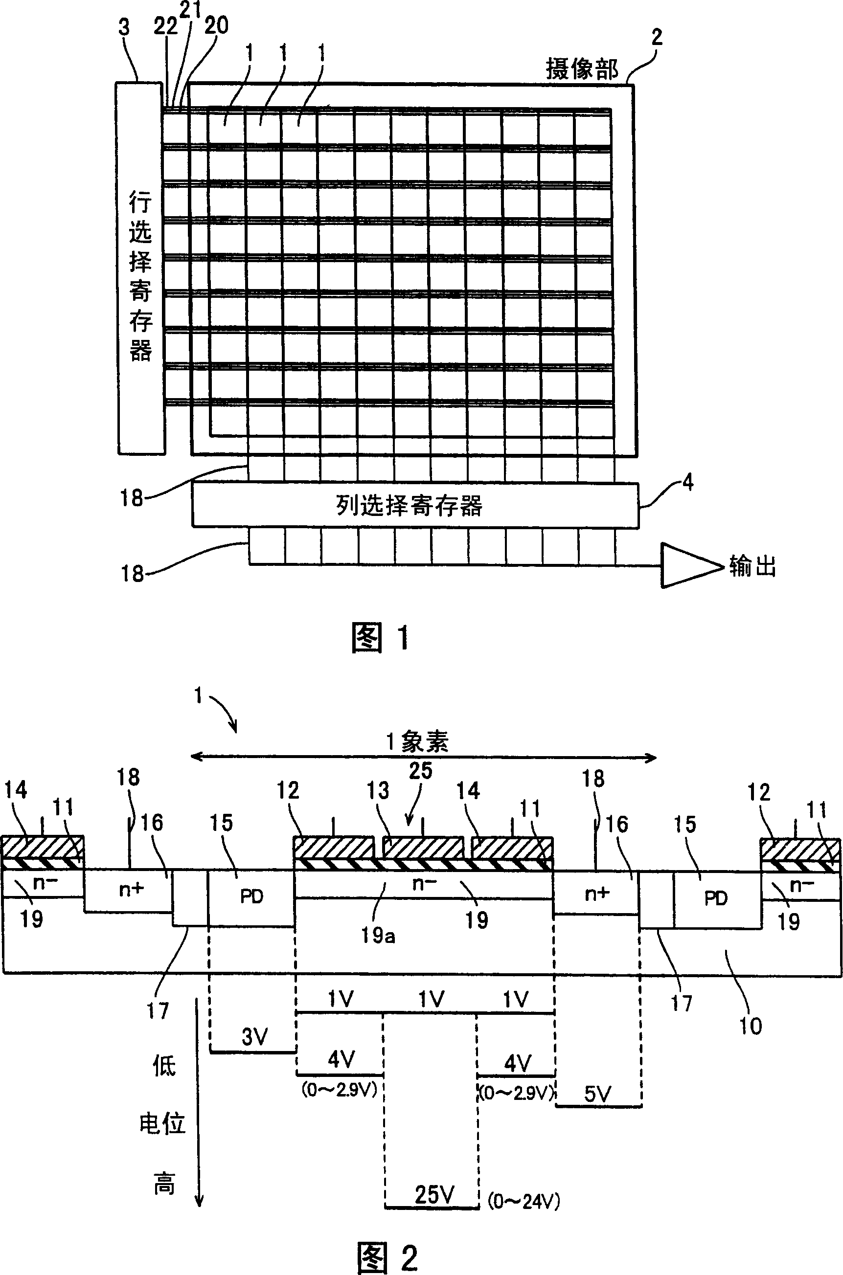
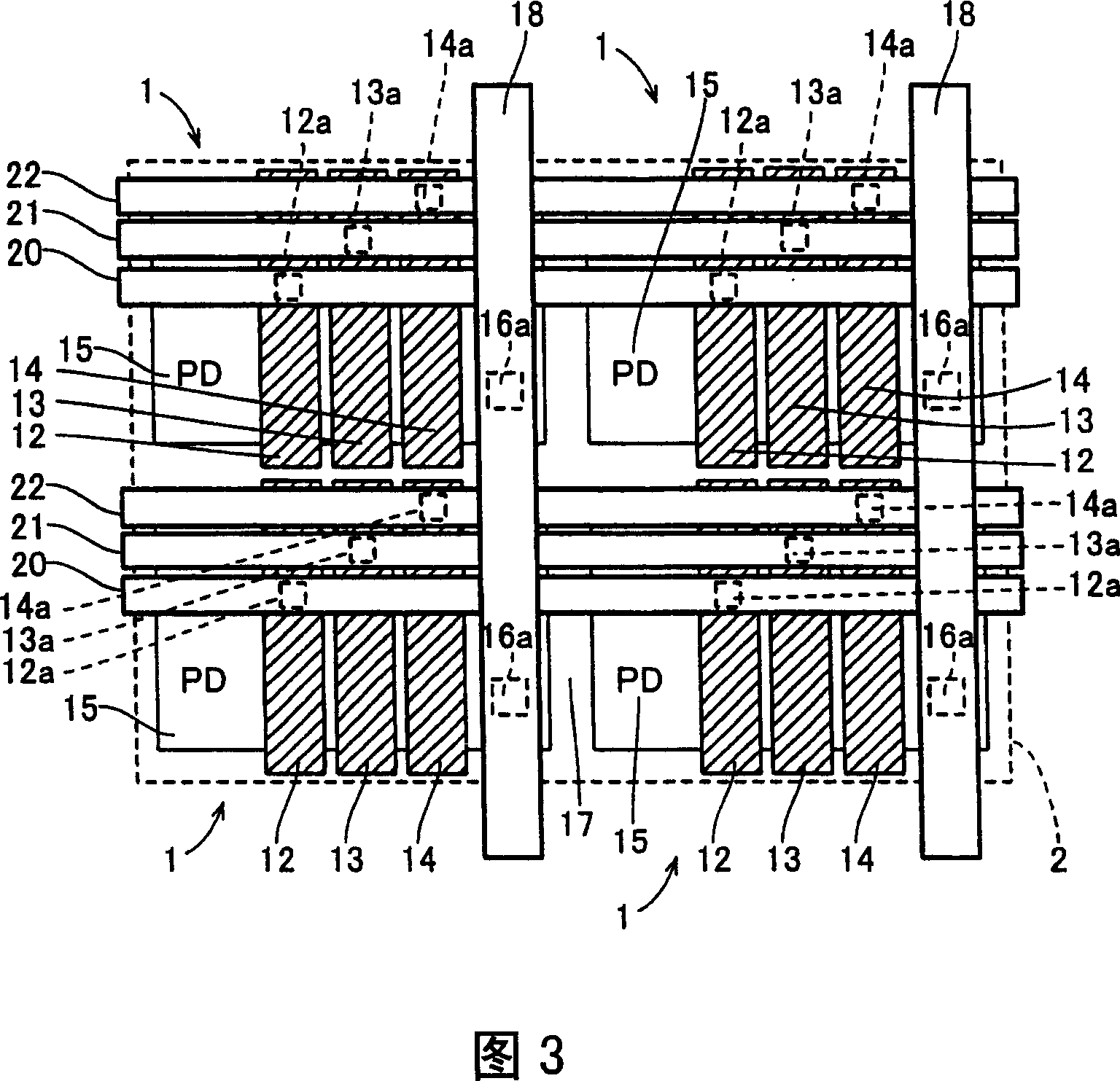
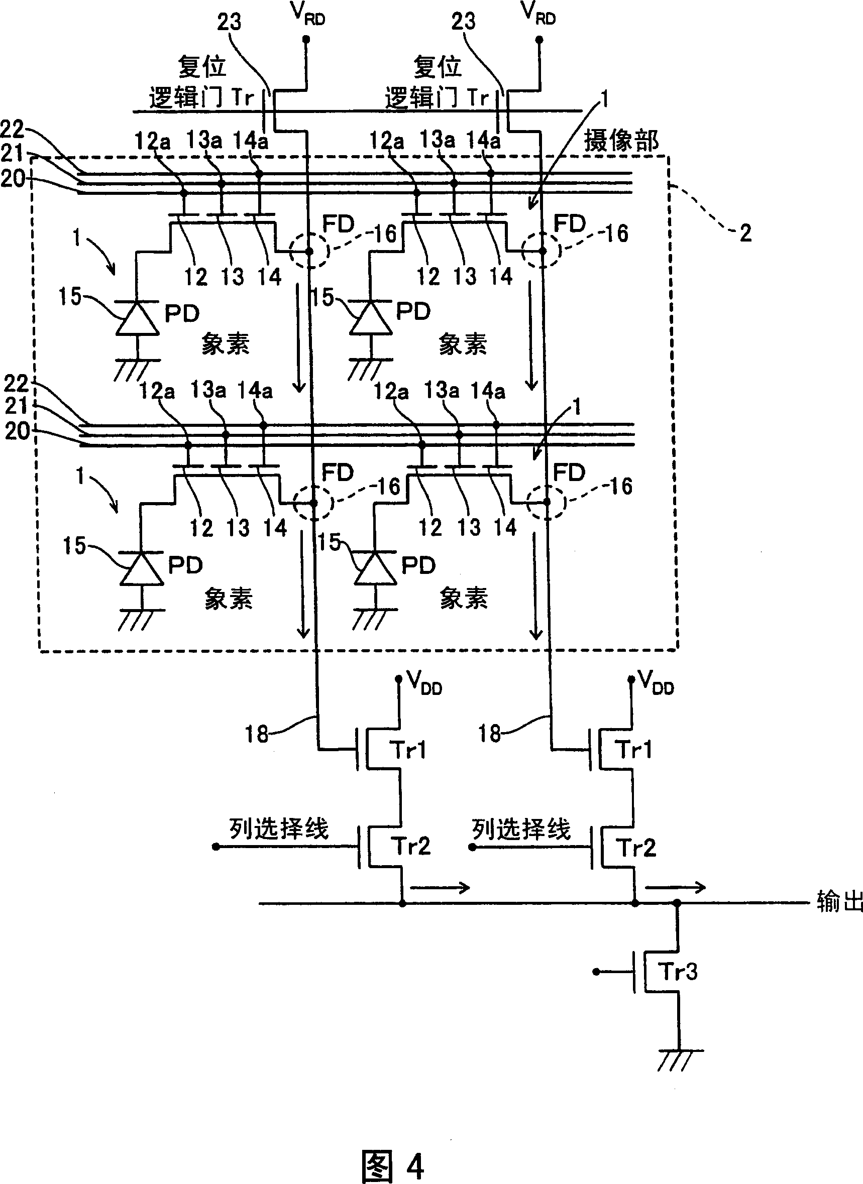
[0046] First, the structure of the CMOS image sensor according to the first embodiment will be described with reference to FIGS. 1 to 4 .

[0047] As shown in FIG. 1 , the CMOS image sensor according to the first embodiment includes an imaging unit 2 including a plurality of pixels 1 , a row selection register 3 , and a column selection register 4 . In addition, as shown in FIG. 2 , the pixel 1 has three gate electrodes: a p-type silicon substrate 10 , a gate insulating film 11 , a transfer gate electrode 12 , a multiplication gate electrode 13 and a readout gate electrode 14 . polar electrode, a photodiode portion (PD) 15 , a floating diffusion region 16 composed of an n-type impurity region, and an element isolation region 17 . In addition, gate insulating film 11 is formed on the surface of p-type silicon substrate 10 at predetermined intervals. In addition, the transfer gate electrode 12 , the doubler gate electrode 13 , and the readout gate electrode 14 are formed in pre...

no. 2 approach

[0069] Referring to FIG. 9 , the configuration of a CMOS image sensor including pixels 30 formed such that photodiode portions 15 are adjacent to readout gate electrodes 14 in the second embodiment, which is different from the first embodiment described above, will be described.

[0070] The cross-sectional structure of the pixel 30 of the CMOS image sensor according to the second embodiment is as shown in FIG. In addition, on the surface of the p-type silicon substrate 10 of each pixel 30 surrounded by the element isolation region 17, a transfer groove composed of an n-type impurity region is sandwiched at a predetermined interval from one side of the element isolation region 17. In the form of the track 31, the photodiode portion 15 is formed. In addition, on the surface of the p-type silicon substrate 10 of each pixel 30, a floating diffusion is formed at a predetermined interval from the photodiode portion 15 so as to sandwich the transfer channel 32 composed of an n-type ...

no. 3 approach

[0083] Referring to FIG. 11 , the structure of a CMOS image sensor including a pixel 40 in which a transfer gate electrode 42 is formed on a photodiode portion 15 in this third embodiment, which is different from the above-mentioned first embodiment, will be described.

[0084]The cross-sectional structure of the pixel 40 of the CMOS image sensor according to the third embodiment, as shown in FIG. Film 41. A transfer gate electrode 42 is formed in a region corresponding to the photodiode portion 15 on the upper surface of the gate insulating film 41 . In addition, the transfer gate electrode 42 is an example of the "second transfer electrode" of this invention. In addition, in a region corresponding to the transfer channel 19 on the upper surface of the gate insulating film 41, the transfer gate electrode 12, the multiplication gate electrode 13, and the readout gate electrode 12 are sequentially formed at predetermined intervals from the photodiode portion 15 side. electrod...


PUM


Abstract

The invention provides an imaging device. The imaging device includes a carrier storage portion for storing carriers generated by photoelectric conversion, having a photoelectric conversion function, a multiplier section including a multiplier electrode applying an electric field for multiplying carriers due to impact ionization by an electric field, one first transfer electrode so provided between the carrier storage portion and the multiplier electrode as to be adjacent to the carrier storage portion and the multiplier electrode. Thereby, the present invention provides an imaging device capable of multiplying carriers and miniaturizing the device.

Description

technical field [0001] The present invention relates to an imaging device, and more particularly to an imaging device including a multiplication unit for multiplying electrons. Background technique [0002] Conventionally, a CCD (Charge Coupled Device) image sensor (imaging device) including a multiplication unit for multiplying electrons has been known. Such a CCD image sensor is disclosed in Japanese Patent No. 3483261, for example. [0003] FIG. 12 is a cross-sectional view showing the structure of a conventional CCD image sensor disclosed in Japanese Patent No. 3483261. First, referring to FIG. 12 , in a conventional CCD image sensor, a gate oxide 102 is formed on the surface of a silicon substrate 101 . In addition, four gate electrodes 103 to 106 are provided at predetermined intervals in predetermined regions on the upper surface of gate oxide 102 . It is configured to supply four-phase clock signals Φ1 to Φ4 to the gate electrodes 103 to 106 . In addition, in the...

Claims


Application Information

Patent Timeline
IPC IPC(8): H01L27/146
Inventor 小田真弘
Owner SANYO ELECTRIC CO LTD
Learn More