Exposure head and an image forming apparatus
An exposure head and image technology, which is applied in the fields of electric recording process applying charge pattern, optics, equipment of electric recording process applying charge pattern, etc., can solve the problems of lower resolution, inability to obtain resolution, and larger lens pitch.
- Summary
- Abstract
- Description
- Claims
- Application Information
AI Technical Summary
Problems solved by technology
Method used
Image
Examples
no. 1 approach
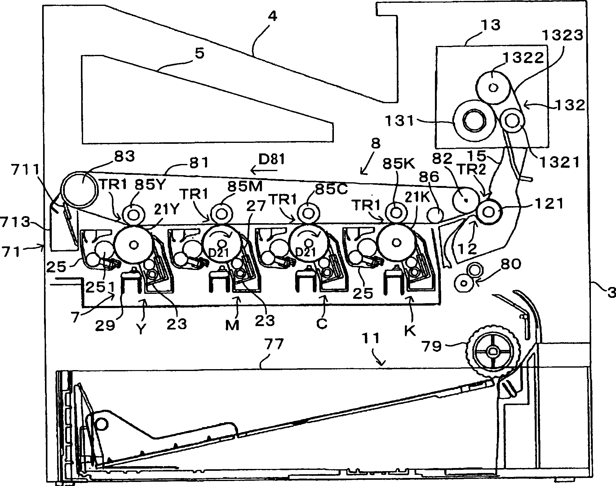
[0073] image 3 It is a diagram showing an example of an image forming apparatus equipped with a line head to which the present invention is applied. in addition, Figure 4yes means image 3 A diagram of the electrical configuration of the image forming apparatus. This device is an image forming device capable of selectively executing a color mode and a monochrome mode in which four colors of black (K), cyan (C), magenta (M), and yellow (Y) are combined. The monochrome mode is a mode in which only black (K) toner is used to form a monochrome image. also, image 3 It is a figure corresponding to the execution of the color mode. In this image forming apparatus, when an image forming command is given from an external device such as a host computer to a main controller MC having a CPU, a memory, etc., the main controller MC gives a control signal and the like to an engine controller EC, and sends a The HC gives video data VD corresponding to the image forming command. In ad...
no. 3 approach
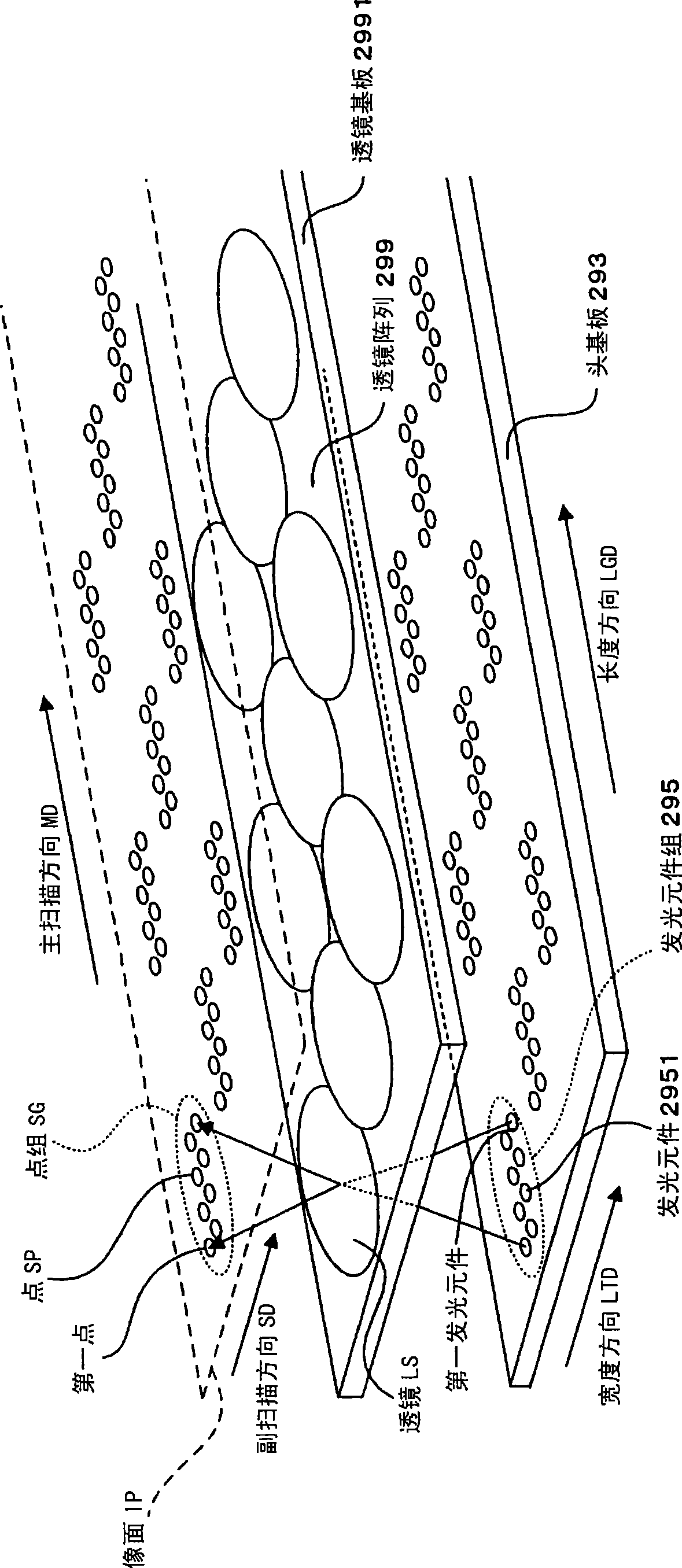
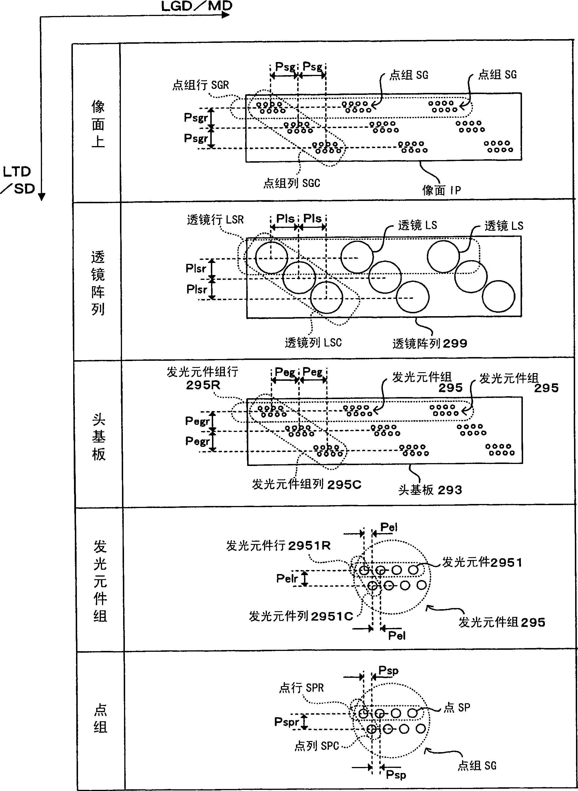
[0124] In addition, in Figure 14In the shown structure, the lens LS-u (first lens, second lens) and the lens LS-m (third lens) are connected to each other, the distance between the lens LS-u and the lens LS-m will not be enlarged, and the lens LS-u can be connected to the lens. A lot of light is incident. In addition, lens LS-m (first lens, second lens) and lens LS-d (third lens) are connected to each other, and a large amount of light can enter the lens without increasing the distance between lens LS-m and lens LS-d. In other words, Figure 14 The structure is a structure capable of suppressing the width of the lens array 299 in the width direction LTD (second direction). As a result, space saving can also be achieved in the width direction LTD in the area where the light emitting elements 2951 are arranged corresponding to the lenses LS on the head substrate 293 . Therefore, in the head substrate 293 on which the light emitting element 2951 is arranged, spaces can be lef...
PUM
| Property | Measurement | Unit |
|---|---|---|
| Thickness | aaaaa | aaaaa |
Abstract
Description
Claims
Application Information


